|
|
|
PDF XR20V2172 Data sheet ( Hoja de datos )
| Número de pieza | XR20V2172 | |
| Descripción | TWO CHANNEL I2C/SPI UART | |
| Fabricantes | Exar Corporation | |
| Logotipo | ||
Hay una vista previa y un enlace de descarga de XR20V2172 (archivo pdf) en la parte inferior de esta página. Total 30 Páginas | ||
|
No Preview Available !
www.DataSheet4U.com
PRELIMINARY
XR20V2172
TWO CHANNEL I2C/SPI UART WITH 64-BYTE FIFO AND RS232 TRANSCEIVER
FEBRUARY 2007
REV. P1.0.1
GENERAL DESCRIPTION
The XR20V21721 (V2172) is a high performance two
channel universal asynchronous receiver and
transmitter (UART) with 64 byte TX and RX FIFOs, a
selectable I2C/SPI slave interface and RS232
transceiver. The V2172 operates from 3.3 to 5.5 volts.
The enhanced features in the V2172 include a
programmable fractional baud rate generator, an 8X
and 4X sampling rate that allows for a maximum baud
rate of 1 Mbps at 3.3V. The standard features include
16 selectable TX and RX FIFO trigger levels,
automatic hardware (RTS/CTS) and software (Xon/
Xoff) flow control, and a complete modem interface.
Onboard registers provide the user with operational
status and data error flags. An internal loopback
capability allows system diagnostics. The V2172 is
available in the 64-pin QFN.
NOTE: 1 Covered by U.S. Patent #5,649,122
APPLICATIONS
• Portable Appliances
• Battery-Operated Devices
• Cellular Data Devices
• Factory Automation and Process Controls
FEATURES
• Selectable I2C/SPI Interface
• Meets true EIA/TIA-232-F Standards from +3.3V to
+5.5V operation
• Data rate up to 1 Mbps
• 45us sleep mode exit (charge pump to full power)
• ESD protection for RS-232 I/O pins at
■ +/-15kV - Human Body Model
■ +/-15kV - IEC 1000-4-2, Air-Gap Discharge
■ +/- 8kV - IEC 1000-4-2, Contact Discharge
• Full-featured UART
■ Fractional Baud Rate Generator
■ Transmit and Receive FIFOs of 64 bytes
■ 16 Selectable TX and RX FIFO Trigger Levels
■ Automatic Hardware (RTS/CTS) Flow Control
■ Automatic Software (Xon/Xoff) Flow Control
■ Halt and Resume Transmission Control
■ Automatic sleep mode
■ General Purpose I/Os
■ Full modem interface
• 64-QFN packages
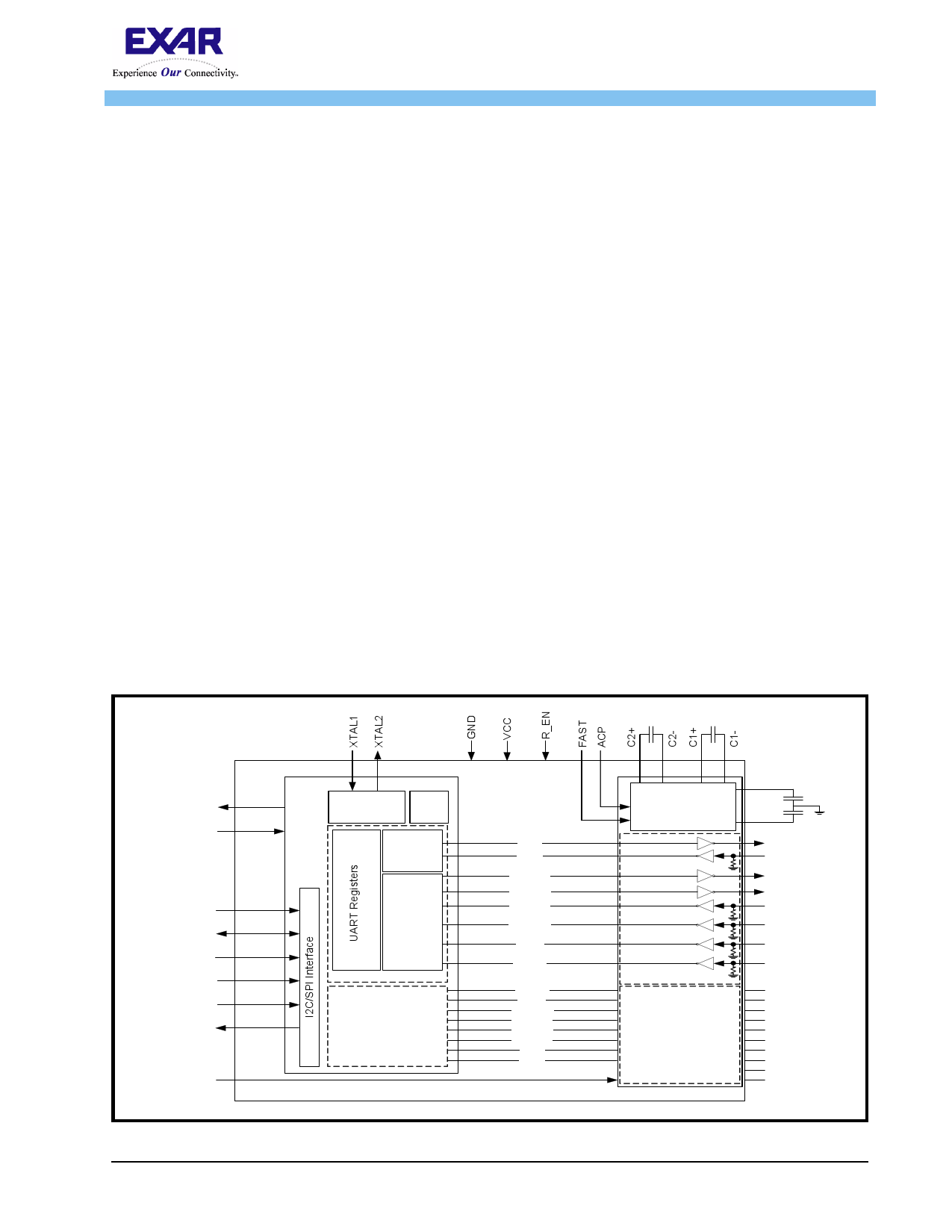
FIGURE 1. XR20V2172 BLOCK DIAGRAM
IR Q #
RESET#
I2 C /S P I#
SDA
SCK
A 0 /C S A #
A 1 /S I
SO
RXB_SEL
C rys ta l
O sc /B u ffe r
BRG
64 Byte
TX & RX
FIFO
Modem
I/O s
Channel A
Channel B
UART
TXA
RXA
RTSA#
DTRA#
CTSA#
DSRA#
R IA #
CDA#
CDB#
R IB #
DSRB#
CTSB#
DTRB#
RTSB#
TXB
RXB
Charge Pump
5K
5K
5K
5K
C h A T ra n sc e iv e r5K
Channel B
T ra n s c e iv e r
R S-232 Transceiver
VREF+
VREF-
TXDA
RXDA
RTSA
DTRA
CTSA
DSRA
R IA
CDA
CDB
R IB
DSRB
CTSB
DTRB
RTSB
TXDB
RXDB
TXB
RXB
Exar Corporation 48720 Kato Road, Fremont CA, 94538 • (510) 668-7000 • FAX (510) 668-7017 • www.exar.com
1 page 
REV. P1.0.1
Pin Description
PRELIMINARY
XR20V2172
TWO CHANNEL I2C/SPI UART WITH 64-BYTE FIFO AND RS232 TRANSCEIVER
NAME
NC
64-QFN
PIN #
3, 9, 10, 11, 18,
22, 23, 26, 30,
31, 32, 34, 35,
37, 46, 47, 48,
49, 55
TYPE
-
No Connection.
DESCRIPTION
NOTE: Pin type: I=Input, O=Output, I/O= Input/output, OD=Output Open Drain. For CMOS/TTL Voltage levels, ’LOW’
indicates a voltage in the range 0V to VIL and ’HIGH" indicates a voltage in the range VIH to VCC. For RS-232
input voltage levels, ’LOW’ is any voltage < -3V and ’HIGH’ is any voltage > 3V. For RS-232 output voltage levels,
’LOW’ is any voltage < -5V and ’HIGH’ is any voltage > 5V.
5
5 Page 
REV. P1.0.1
PRELIMINARY
XR20V2172
TWO CHANNEL I2C/SPI UART WITH 64-BYTE FIFO AND RS232 TRANSCEIVER
TABLE 5: IRQ# PIN OPERATION FOR RECEIVER
IRQ# Pin
FCR BIT-0 = 0
(FIFO DISABLED)
HIGH = no data
LOW = 1 byte
FCR BIT-0 = 1
(FIFO ENABLED)
HIGH = FIFO below trigger level
LOW = FIFO above trigger level
2.6 Crystal Oscillator or External Clock Input
The V2172 includes an on-chip oscillator (XTAL1 and XTAL2) to produce a clock for both UART sections in the
device. The CPU data bus does not require this clock for bus operation. The crystal oscillator provides a
system clock to the Baud Rate Generators (BRG) section found in each of the UART. XTAL1 is the input to the
oscillator or external clock buffer input with XTAL2 pin being the output. Please note that the input XTAL1 is not
5V tolerant and so the maximum at the pin should be VCC. For programming details, see ““Section 2.7,
Programmable Baud Rate Generator with Fractional Divisor” on page 11.”
FIGURE 7. TYPICAL OSCILLATOR CONNECTIONS
XTAL1
XTAL2
R2
500 ΚΩ− 1 ΜΩ
R1
0-120 Ω
(Optional)
C1
22-47 pF
Y1
1.8432 MHz
to
24 MHz
C2
22-47 pF
The on-chip oscillator is designed to use an industry standard microprocessor crystal (parallel resonant,
fundamental frequency with 10-22 pF capacitance load, ESR of 20-120 ohms and 100 ppm frequency
tolerance) connected externally between the XTAL1 and XTAL2 pins (see Figure 7). The programmable Baud
Rate Generator is capable of operating with a crystal oscillator frequency of up to 24 MHz. Although the V2172
can accept an external clock of up to 64MHz, the maximum data rate supported by the RS-232 drivers is
250Kbps. For further reading on the oscillator circuit please see the Application Note DAN108 on the EXAR
web site at http://www.exar.com.
2.7 Programmable Baud Rate Generator with Fractional Divisor
Each UART has its own Baud Rate Generator (BRG) with a prescaler for the transmitter and receiver. The
prescaler is controlled by a software bit in the MCR register. The MCR register bit-7 sets the prescaler to divide
the input crystal or external clock by 1 or 4. The output of the prescaler clocks to the BRG. The BRG further
divides this clock by a programmable divisor between 1 and (216 - 0.0625) in increments of 0.0625 (1/16) to
obtain a 16X, 8X or 4X sampling clock of the serial data rate. The sampling clock is used by the transmitter for
data bit shifting and receiver for data sampling. The BRG divisor (DLL, DLM and DLD registers) defaults to the
11
11 Page | ||
| Páginas | Total 30 Páginas | |
| PDF Descargar | [ Datasheet XR20V2172.PDF ] | |
Hoja de datos destacado
| Número de pieza | Descripción | Fabricantes |
| XR20V2170 | I2C/SPI UART | Exar Corporation |
| XR20V2172 | TWO CHANNEL I2C/SPI UART | Exar Corporation |
| Número de pieza | Descripción | Fabricantes |
| SLA6805M | High Voltage 3 phase Motor Driver IC. |
Sanken |
| SDC1742 | 12- and 14-Bit Hybrid Synchro / Resolver-to-Digital Converters. |
Analog Devices |
|
DataSheet.es es una pagina web que funciona como un repositorio de manuales o hoja de datos de muchos de los productos más populares, |
| DataSheet.es | 2020 | Privacy Policy | Contacto | Buscar |