|
|
|
PDF XRT91L81 Data sheet ( Hoja de datos )
| Número de pieza | XRT91L81 | |
| Descripción | 2.488/2.666GBPS OC-48/STM-16 SONET/SDH TRANSCEIVER | |
| Fabricantes | Exar Corporation | |
| Logotipo | ||
Hay una vista previa y un enlace de descarga de XRT91L81 (archivo pdf) en la parte inferior de esta página. Total 30 Páginas | ||
|
No Preview Available !
www.DataSheet4U.com
PRELIMINARY
XRT91L81
JANUARY 2004
2.488/2.666GBPS OC-48/STM-16 SONET/SDH TRANSCEIVER
REV. P1.0.3
GENERAL DESCRIPTION
The XRT91L81 is a fully integrated SONET/SDH
transceiver block for applications in SONET OC-48
allowing the use of Forward Error Correction (FEC)
capability. The transceiver includes an on-chip Clock
Multiplier Unit (CMU), which uses a high frequency
Phase-Locked Loop (PLL) to generate the high-
speed transmit serial clock from slower external clock
references. It also provides Clock and Data Recovery
(CDR) functions by synchronizing its on-chip Voltage
Controlled Oscillator (VCO) to the incoming serial
data stream. The chip provides serial-to-parallel and
parallel-to-serial converters and 4-bit LVDS system
interfaces in both receive and transmit directions.
The transmit section includes a 4x9 Elastic Buffer
(FIFO) to absorb any phase differences between the
transmitter input clock and the internally generated
transmitter reference clock. In the event of an
overflow, an internal FIFO control circuit outputs an
OVERFLOW indication. The FIFO under the control
of the AUTORST pin can automatically recover from
an overflow condition. The operation of the device
can be monitored by checking the status of the
LOCKDET and LOSDET output signals. An on-chip
phase/frequency detector and charge-pump offers
the ability to form a de-jittering PLL with an external
VCXO that can be used in loop timing mode to clean
up the recovered clock in the receive section.
APPLICATIONS
• SONET/SDH-based Transmission Systems
• Add/Drop Multiplexers
• Cross Connect Equipment
• ATM and Multi-Service Switches, Routers and
Switch/Routers
• DSLAMS
• SONET/SDH Test Equipment
• DWDM Termination Equipment
• Optical Modules and Sub-Systems
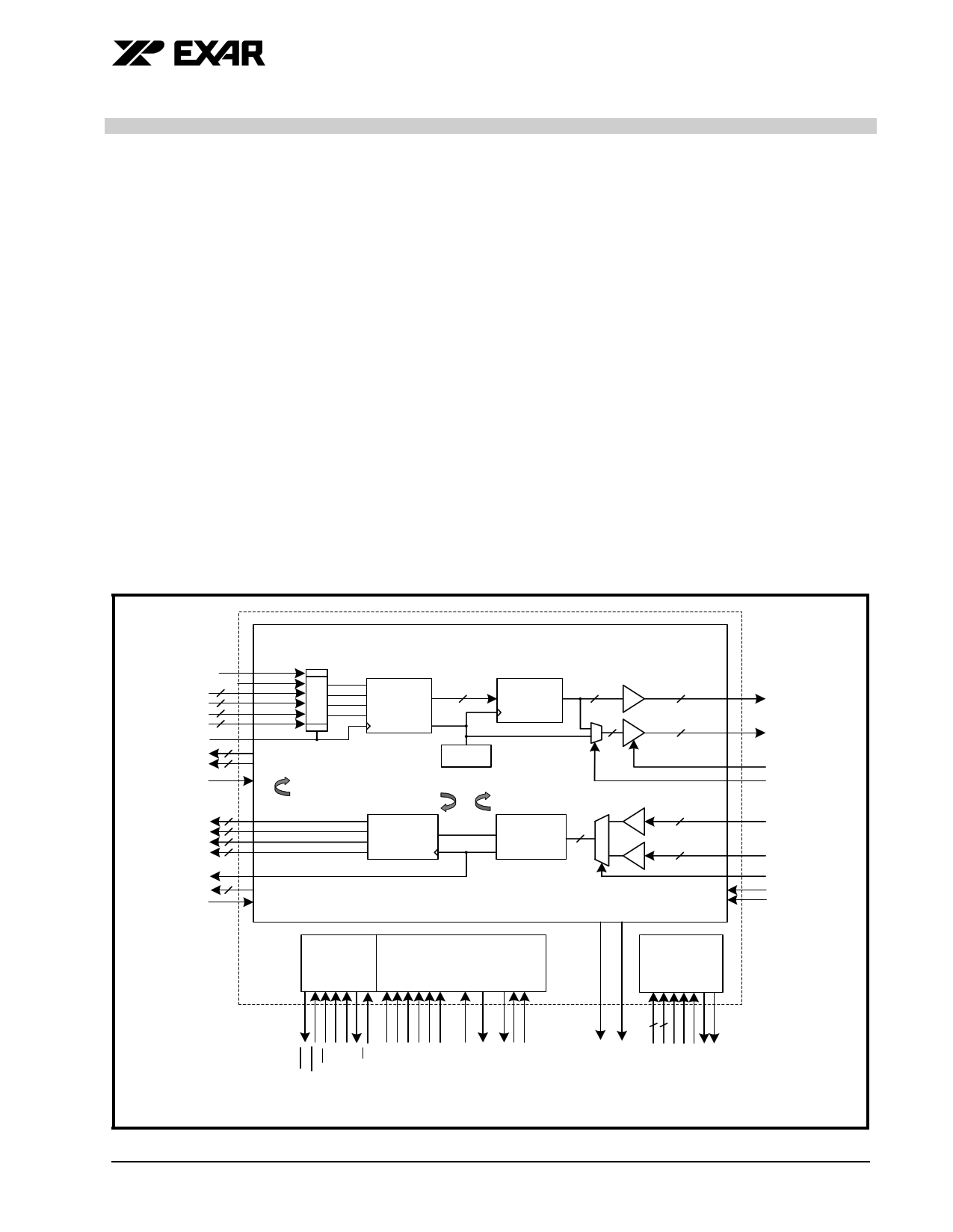
FIGURE 1. BLOCK DIAGRAM OF THE XRT91L81
FIFO_RST
FIFO_AUTORST
TxDI0P/N
TxDI1P/N
TxDI2P/N
TxDI3P/N
TxCLKIP/N
TXPCLKOP/N
TXCLKO16P/N
TRITXCLKO16
OC-48 TRANSCEIVER
WP
RP
RLOOPP
PISO
(Parallel Input
Serial Output)
Re-Timer
CMU
DLOOP RLOOPS
RxDO0P/N
RxDO1P/N
RxDO2P/N
RxDO3P/N
RxCLKP/N
RXCLK16P/N
DISRD
SIPO
(Serial Input
Parallel Output)
CDR
0
1
0
1
Serial
Microprocessor
Hardware
Control
PFD
& Charge Pump
TXOP/N
TXO2P/N
TXO2DIS
TXO2SEL
RXI0P/N
RXI1P/N
RXSEL
TRIRXD
REXT
Exar Corporation 48720 Kato Road, Fremont CA, 94538 • (510) 668-7000 • FAX (510) 668-7017 • www.exar.com
1 page 
PRELIMINARY
XRT91L81
2.488/2.666GBPS OC-48/STM-16 SONET/SDH TRANSCEIVER
REV. P1.0.3
FIGURE 15. PARALLEL REMOTE LOOPBACK .................................................................................................................................... 23
4.3 DIGITAL LOCAL LOOPBACK ....................................................................................................................... 24
FIGURE 16. DIGITAL LOOPBACK...................................................................................................................................................... 24
4.4 SONET JITTER REQUIREMENTS ................................................................................................................. 25
4.4.1 JITTER TOLERANCE: ................................................................................................................................................ 25
FIGURE 17. JITTER TOLERANCE MASK............................................................................................................................................ 25
4.4.2 JITTER TRANSFER .................................................................................................................................................... 26
4.4.3 JITTER GENERATION................................................................................................................................................ 26
5.0 SERIAL MICROPROCESSOR INTERFACE BLOCK ......................................................................... 27
FIGURE 18. SIMPLIFIED BLOCK DIAGRAM OF THE SERIAL MICROPROCESSOR INTERFACE ................................................................. 27
5.1 SERIAL TIMING INFORMATION ................................................................................................................... 27
FIGURE 19. TIMING DIAGRAM FOR THE SERIAL MICROPROCESSOR INTERFACE ................................................................................ 27
5.2 16-BIT SERIAL DATA INPUT DESCRITPTION ............................................................................................. 28
5.2.1 R/W (SCLK1)............................................................................................................................................................... 28
5.2.2 A[5:0] (SCLK2 - SCLK7)............................................................................................................................................. 28
5.2.3 X (DUMMY BIT SCLK8) .............................................................................................................................................. 28
5.2.4 D[7:0] (SCLK9 - SCLK16)........................................................................................................................................... 28
5.3 8-BIT SERIAL DATA OUTPUT DESCRIPTION ............................................................................................. 28
6.0 REGISTER MAP AND BIT DESCRIPTIONS ....................................................................................... 29
TABLE 7: MICROPROCESSOR REGISTER BIT DESCRIPTION .............................................................................................................. 29
TABLE 6: MICROPROCESSOR REGISTER MAP.................................................................................................................................. 29
TABLE 9: MICROPROCESSOR REGISTER BIT DESCRIPTION .............................................................................................................. 30
TABLE 8: MICROPROCESSOR REGISTER BIT DESCRIPTION .............................................................................................................. 30
TABLE 10: MICROPROCESSOR REGISTER BIT DESCRIPTION ............................................................................................................ 31
TABLE 11: MICROPROCESSOR REGISTER BIT DESCRIPTION ............................................................................................................ 33
TABLE 12: MICROPROCESSOR REGISTER BIT DESCRIPTION ............................................................................................................ 34
TABLE 13: MICROPROCESSOR REGISTER 0X02H BIT DESCRIPTION ................................................................................................. 35
TABLE 14: MICROPROCESSOR REGISTER 0X01H BIT DESCRIPTION ................................................................................................. 35
7.0 ELECTRICAL CHARACTERISTICS ................................................................................................... 36
ABSOLUTE MAXIMUMS ................................................................................................................................. 36
DC ELECTRICAL CHARACTERISTICS.............................................................................................................. 36
196 SHRINK THIN BALL GRID ARRAY ................................................................................................. 37
(12.0 MM X 12.0 MM, STBGA).......................................................................................................... 37
REV. 1.00 ......................................................................................................................................... 37
ORDERING INFORMATION .................................................................................................................. 37
REVISION HISTORY ...................................................................................................................................... 38
II
5 Page 
PRELIMINARY
RECEIVER SECTION
NAME
LEVEL
RXI0P
RXI0N
CMLDIFF
TYPE
I
RXI1P
RXI1N
CMLDIFF
I
RXSEL
LVTTL
I
REXT
-
RXCLK16P
RXCLK16N
LVDS
LOCKDET_CDR
LVTTL
LOSEXT
POLARITY
LVTTL
LVTTL
I
O
O
I
I
LOSDET
LVTTL
O
DISRD
LVTTL
I
XRT91L81
2.488/2.666GBPS OC-48/STM-16 SONET/SDH TRANSCEIVER
REV. P1.0.3
PIN DESCRIPTION
C1 Primary Receive Serial Data Input
D1 The receive serial data stream of 2.488Gbps is applied to the
primary input pins if RXSEL is "Low". In Forward Error Correc-
tion, the receive serial data stream is 2.666Gbps.
G1 Secondary Receive Serial Data Input Port
F1 The receive serial data stream of 2.488Gbps is applied to the
secondary input pins if RXSEL is "High". In Forward Error Cor-
rection, the receive serial data stream is 2.666Gbps.
A2 Receive Serial Data Select
Hardware Mode This pin is used to select the Receive Serial
Data Input from the primary or secondary inputs.
"Low" = RXI0
"High" = RXI1
A1 Limiting Amplifier Biasing Resistor
This pin should be pulled "Low" with a 499Ω resistor.
A6 155.52 (166) MHz Reference Clock
A7 This output clock reference is derived from the recovered clock
from the receive path.
C7 CDR Lock Detect
This pin will be pulled "High" to indicate that the CDR is locked.
B5 LOS or SD input from optical module
C4 Polarity for LOS input
Hardware Mode LOSEXT and POLARITY signals will be
Exclussive NORed internally to generate the correct polarity.
C5 LOS Detect
Flags LOS condition based on LOS/SD signal from optical
module.
A3 Disable Receive Output Data Upon LOS
Hardware Mode If this pin is pulled "High", the receive output
data will automically pull "Low" when a LOS condition occurs.
"Low" = Disabled
"High" = Mute Data Upon LOS
9
11 Page | ||
| Páginas | Total 30 Páginas | |
| PDF Descargar | [ Datasheet XRT91L81.PDF ] | |
Hoja de datos destacado
| Número de pieza | Descripción | Fabricantes |
| XRT91L80 | 2.488/2.666 GBPS STS-48/STM-16 SONET/SDH TRANSCEIVER | Exar Corporation |
| XRT91L81 | 2.488/2.666GBPS OC-48/STM-16 SONET/SDH TRANSCEIVER | Exar Corporation |
| XRT91L82 | 2.488/2.666 GBPS STS-48/STM-16 SONET/SDH TRANSCEIVER | Exar Corporation |
| Número de pieza | Descripción | Fabricantes |
| SLA6805M | High Voltage 3 phase Motor Driver IC. |
Sanken |
| SDC1742 | 12- and 14-Bit Hybrid Synchro / Resolver-to-Digital Converters. |
Analog Devices |
|
DataSheet.es es una pagina web que funciona como un repositorio de manuales o hoja de datos de muchos de los productos más populares, |
| DataSheet.es | 2020 | Privacy Policy | Contacto | Buscar |