|
|
|
PDF XRK7933 Data sheet ( Hoja de datos )
| Número de pieza | XRK7933 | |
| Descripción | INTELLIGENT DYNAMIC CLOCK SWITCH PLL CLOCK DRIVER | |
| Fabricantes | Exar Corporation | |
| Logotipo | ||
Hay una vista previa y un enlace de descarga de XRK7933 (archivo pdf) en la parte inferior de esta página. Total 10 Páginas | ||
|
No Preview Available !
xrwww.DataSheet4U.com
PRELIMINARY
XRK7933
INTELLIGENT DYNAMIC CLOCK SWITCH PLL CLOCK DRIVER
MARCH 2005
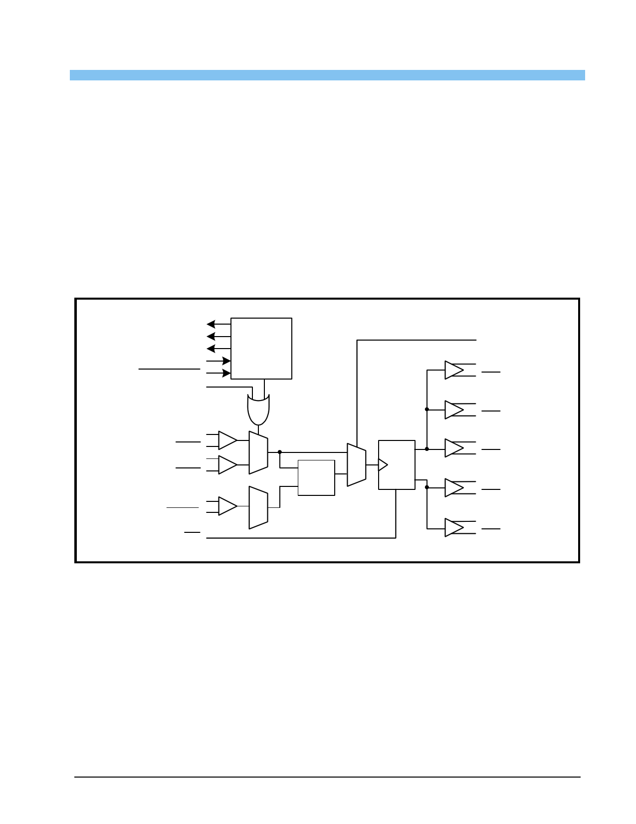
GENERAL DESCRIPTION
The XRK7933 is a PLL clock driver designed
specifically for redundant clock tree designs. The
device receives two differential LVPECL clock signals
from which it generates 5 new differential LVPECL
clock outputs. Two of the output pairs regenerate the
input signals frequency and phase while the other
three pairs generate 3x, phase aligned clock outputs.
External PLL feedback is used to also provide zero
delay buffer performance.
The XRK7933 Intelligent Dynamic Clock Switch
circuit continuously monitors both input CLK signals.
Upon detection of a failure (CLK stuck HIGH or LOW
for at least 1 period), the INP_BAD for that CLK will
REV. P1.0.1
be latched (H). If that CLK is the primary clock, the
device will switch to the good secondary clock and
phase/frequency alignment will occur with minimal
output phase disturbance. The typical phase bump
caused by a failed clock is eliminated.
FEATURES
• Fully Integrated PLL
• Intelligent Dynamic Clock Switch
• LVPECL Clock Outputs
• LVCMOS Control I/O
• 3.3V Operation
• 32-Lead LQFP Packaging
FIGURE 1. BLOCK DIAGRAM OF THE XRK7933
CLK_Selected
INP1Bad
INP0Bad
Man_Override
Alarm_Reset
Sel_CLK
CLK0
CLK0
CLK1
CLK1
Ext_FB
Ext_FB
MR
Dynamic
Switch
Logic
OR
PLL
200-400MHz
÷4
÷12
PLL_En
Qb0
Qb0
Qb1
Qb1
Qb2
Qb2
Qa0
Qa0
Qa1
Qa1
Exar Corporation 48720 Kato Road, Fremont CA, 94538 • (510) 668-7000 • FAX (510) 668-7017 • www.exar.com
1 page 
XRK7933
PRELIMINARY
INTELLIGENT DYNAMIC CLOCK SWITCH PLL CLOCK DRIVER
xr
REV. P1.0.1
DC CHARACTERISTICS (VCC= 3.3 + 5%, TA= -40°C TO +85°C)
SYMBOL
CHARACTERISTICS
MIN TYP MAX UNIT CONDITION
LVCMOS control inputs (MR, PLL_En, Sel_CLK, Man_Override, Alarm_Reset)
VIH Input voltage high
2.0 VCC+0.3 V
VIL Input voltage low
0.8 V
IIN Input currenta
100
-150
µΑ VIN =VCC or VIN =GND
LVCMOS Control Outputs
VOH Output High Voltage
2.0
V IOH=-10mA
VOL Output Low Voltage
0.55
V IOL=10mA
LVPECL clock inputs (CLK, CLK)b
IIN Input current
+100
µΑ VIN =VCC or VIN =GND
LVPECL clock outputs (Qa[1:0], Qa[1:0], Qb[2:0], Qb[2:0])
VOH Output high voltage
VCC-1.2
VCC-0.7 V Termination 50Ω to VTT
VOL Output low voltage
VCC-1.9
VCC-1.45 V Termination 50Ω to VTT
Supply Current
IGND Maximum ground supply current - gnd pins
180 mA GND pins
ICCPLL Maximum PLL power supply - VCC_PLL pin
15 mA VCCPLL pin
a. Inputs have internal pullup/pulldown resistors which affect the input current.
b. Clock inputs driven by LVPECL compatible signals.
5
5 Page | ||
| Páginas | Total 10 Páginas | |
| PDF Descargar | [ Datasheet XRK7933.PDF ] | |
Hoja de datos destacado
| Número de pieza | Descripción | Fabricantes |
| XRK7933 | INTELLIGENT DYNAMIC CLOCK SWITCH PLL CLOCK DRIVER | Exar Corporation |
| Número de pieza | Descripción | Fabricantes |
| SLA6805M | High Voltage 3 phase Motor Driver IC. |
Sanken |
| SDC1742 | 12- and 14-Bit Hybrid Synchro / Resolver-to-Digital Converters. |
Analog Devices |
|
DataSheet.es es una pagina web que funciona como un repositorio de manuales o hoja de datos de muchos de los productos más populares, |
| DataSheet.es | 2020 | Privacy Policy | Contacto | Buscar |