|
|
|
PDF XRK39910 Data sheet ( Hoja de datos )
| Número de pieza | XRK39910 | |
| Descripción | 3.3V LOW SKEW PLL CLOCK DRIVER | |
| Fabricantes | Exar Corporation | |
| Logotipo | ||
Hay una vista previa y un enlace de descarga de XRK39910 (archivo pdf) en la parte inferior de esta página. Total 9 Páginas | ||
|
No Preview Available !
www.DataSheet4U.com
JULY 2006
FUNCTIONAL DESCRIPTION
The XRK39910 is a high fanout phase locked-loop
clock driver intended for high performance computing
and data-communications applications. It has eight
zero delay LVTTL outputs.
When the OE pin is held low, all the outputs are syn-
chronously enabled. However, if OE is held high, all
the outputs except Q2 and Q3 are synchronously dis-
abled.
Furthermore, when the PE is held high, all the outputs
are synchronized with the positive edge of the CLKIN.
When PE is held low, all the outputs are synchronized
with the negative edge of CLKIN.
The FB_IN signal is compared with the input CLKIN
signal at the phase detector in order to drive the
VCO. Phase differences cause the VCO of the PLL to
adjust upwards or downwards accordingly.
An internal loop filter moderates the response of the
VCO to the phase detector. The loop filter transfer
function has been chosen to provide minimal jitter (or
frequency variation) while still providing accurate
responses to input frequency changes.
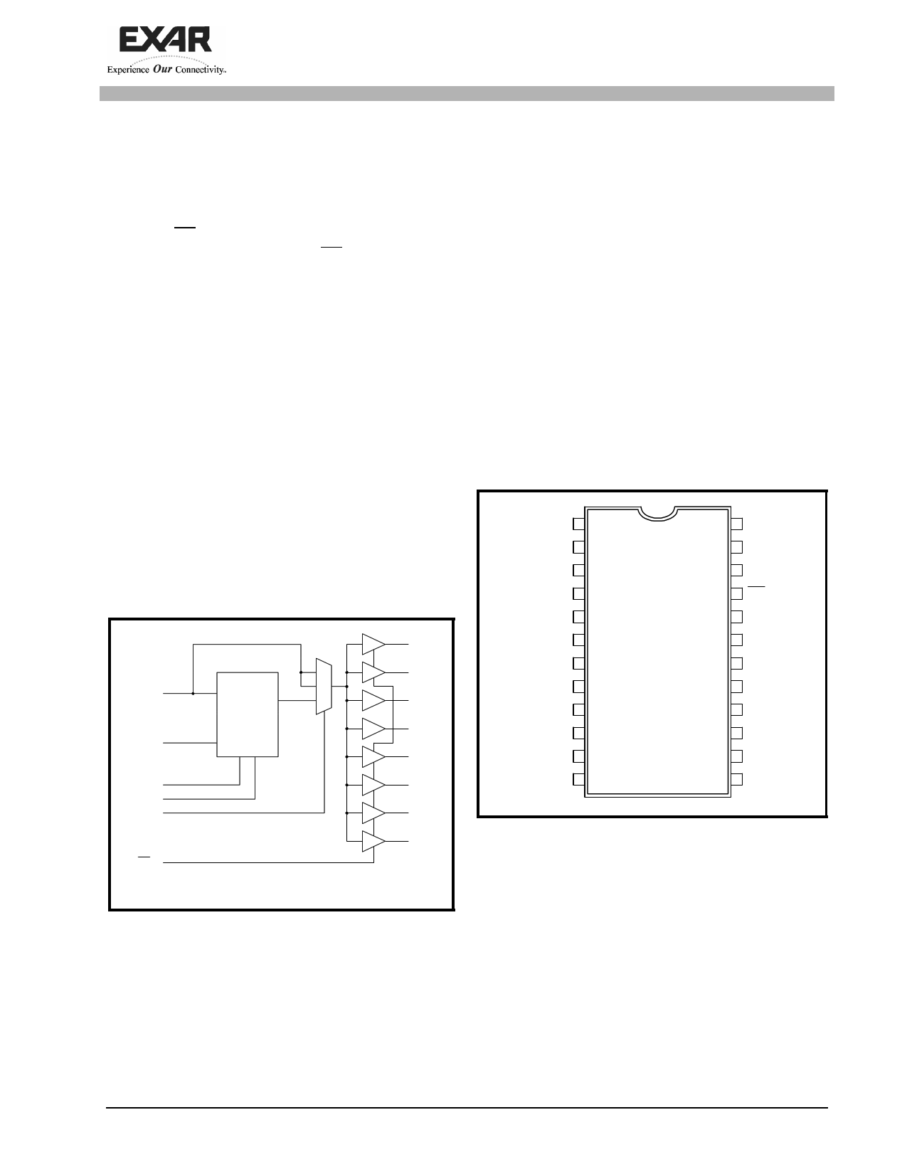
FIGURE 1. FUNCTIONAL BLOCK DIAGRAM
CLKIN
FB_IN
FSEL*
PE
Bypass*
OE
Ref
VCO
PLL
Feedback
H
M
L
* Tri-Level inputs
Q0
Q1
Q2
Q3
Q4
Q5
Q6
Q7
XRK39910
3.3V LOW SKEW PLL CLOCK DRIVER
REV. 1.0.0
FEATURES
• Eight zero delay outputs
• 12mA balanced drive outputs
• Output frequency: 15MHz to 85MHz
• <250ps of output to output skew
• Low Jitter: <200ps peak-to-peak
• 3 skew grades
• External feedback, internal loop filter
• Selectable positive or negative
synchronization
• Synchronous output enable
• 3-level inputs for PLL range control
• PLL bypass for DC testing
• Available in SOIC package
edge
FIGURE 2. PIN CONFIGURATION
CLKIN 1
24 GND
VDDPLL
FSEL
2
3
23 Bypass
22 nc
nc 4
21 OE
PE
VDD
Q0
5
6
7
20 VDD
19 Q7
XRK39910
18 Q6
Q1 8
17 GND
GND 9
16 Q5
Q2 10
15 Q4
Q3
VDD
11
12
14 VDD
13 FB_IN
Exar Corporation 48720 Kato Road, Fremont CA, 94538 • (510) 668-7000 • FAX (510) 668-7017 • www.exar.com
1 page 
REV. 1.0.0
XRK39910
3.3V LOW SKEW PLL CLOCK DRIVER
TABLE 9: SWITCHING CHARACTERISTICS OVER OPERATING RANGE
SYMBOL
PARAMETER
XRK39910-2
XRK39910-5
XRK39910-7
UNIT
MIN TYP MAX MIN TYP MAX MIN TYP MAX
FREF CLKIN Frequency Range FSEL = LOW
15
35 15
35 15
35 MHz
FSEL = MED
25
60 25
60 25
60
FSEL = HIGH
40
85 40
85 40
85
tRPWH CLKIN Pulse Width HIGH
33
3 ns
tRPWL CLKIN Pulse Width LOW
33
3 ns
tSKEW Output Skew (All Outputs) [1, 3, 4]
0.1 0.25
0.25 0.5
0.3 0.75 ns
tDEV Device-to-Device Skew [1, 2, 5]
0.75
1.25
1.65 ns
tPD CLKIN Input to FB_IN Propagation Delay [1, 7] -0.25 0 0.25 -0.5 0 0.5 -0.7 0 0.7 ns
tODCV Output Duty Cycle Variation from 50% [1]
-1.2 0 1.2 -1.2 0 1.2 -1.2 0 1.2 ns
tORISE Output Rise Time [1]
0.15 1 1.2 0.15 1 1.5 0.15 1.5 2.5 ns
tOFALL Output Fall Time [1]
0.15 1 1.2 0.15 1 1.5 0.15 1.5 2.5 ns
tLOCK PLL Lock Time [1,6]
0.5 0.5 0.5 ms
tJR Cycle-to-Cycle Output Jit- RMS
ter [1]
Peak-to-Peak
25 25 25 ps
200 200 200
NOTES:
1. All timing and jitter tolerances apply for FNOM > 25MHz.
2. Skew is the time between the earliest and the latest output transition among all outputs with the specified load.
3. tSKEW is the skew between all outputs. See AC TEST LOADS.
4. For XRK39910-2 tSKEW is measured with CL = 0pF; for CL = 20pF, tSKEW = 0.35ns Max.
5. tDEV is the output-to-output skew between any two devices operating under the same conditions.
6. tLOCK is the time that is required before synchronization is achieved. This specification is valid only after VDD is
stable and within normal operating limits. This parameter is measured from the application of a new signal or
frequency at CLKIN or FB_IN until tPD is within specified limits.
7. tPD is measured with CLKIN input rise and fall times (from 0.8V to 2V ) of 1ns.
5
5 Page | ||
| Páginas | Total 9 Páginas | |
| PDF Descargar | [ Datasheet XRK39910.PDF ] | |
Hoja de datos destacado
| Número de pieza | Descripción | Fabricantes |
| XRK39910 | 3.3V LOW SKEW PLL CLOCK DRIVER | Exar Corporation |
| Número de pieza | Descripción | Fabricantes |
| SLA6805M | High Voltage 3 phase Motor Driver IC. |
Sanken |
| SDC1742 | 12- and 14-Bit Hybrid Synchro / Resolver-to-Digital Converters. |
Analog Devices |
|
DataSheet.es es una pagina web que funciona como un repositorio de manuales o hoja de datos de muchos de los productos más populares, |
| DataSheet.es | 2020 | Privacy Policy | Contacto | Buscar |