|
|
|
PDF XR17C154 Data sheet ( Hoja de datos )
| Número de pieza | XR17C154 | |
| Descripción | 5V PCI BUS QUAD UART | |
| Fabricantes | Exar Corporation | |
| Logotipo | ||
Hay una vista previa y un enlace de descarga de XR17C154 (archivo pdf) en la parte inferior de esta página. Total 30 Páginas | ||
|
No Preview Available !
áçwww.DataSheet4U.com
JUNE 2004
GENERAL DESCRIPTION
The XR17C1541 (154) is a quad PCI Bus Universal
Asynchronous Receiver and Transmitter (UART) with
same package and pin-out as the Exar XR17x158 oc-
tal UARTs. The device is designed to meet today’s
32-bit PCI Bus and high bandwidth requirements in
communication systems. The global interrupt source
register provides a complete interrupt status indica-
tion for all 4 channels to speed up interrupt parsing.
Each UART is independently controlled and has its
own 16C550 compatible 5G register set, transmit and
receive FIFOs of 64 bytes, fully programmable trans-
mit and receive FIFO trigger levels, transmit and re-
ceive FIFO level counters, automatic hardware flow
control with programmable hysteresis, automatic soft-
ware (Xon/Xoff) flow control, IrDA (Infrared Data As-
sociation) encoder/decoder, 8 multi-purpose defin-
able inputs/outputs, and a 16-bit general purpose tim-
er/counter.
NOTE: 1 Covered by U.S. Patents #5,649,122, #5,949,787
APPLICATIONS
• Remote Access Servers
• Ethernet Network to Serial Ports
• Network Management
• Factory Automation and Process Control
• Point-of-Sale Systems
• Multi-port RS-232/RS-422/RS-485 Cards
XR17C154
5V PCI BUS QUAD UART
FEATURES
REV. 1.3.0
• High Performance Quad UART
• PCI Bus 2.2 Target Interface Compliance
• 5V PCI Bus Compliant up to 33MHz Clock
• 32-bit PCI Bus Interface with EEPROM Interface
• A Global Interrupt Source Register for all 4 UARTs
• Data Transfer in Byte, Word and Double-word
• Data Read/Write Burst Operation
• Each UART is independently Controlled with:
• 16C550 Compatible 5G (Fifth Gen Register Set
• 64-byte Transmit and Receive FIFOs
• Transmit and Receive FIFO Level Counters
• Automatic RTS/CTS or DTR/DSR Flow Control
• Automatic Xon/Xoff Software Flow Control
• Automatic RS485 Half-duplex Control Output
with 16 Selectable Turn-around Delay
• Infrared (IrDA 1.0) Data Encoder/Decoder
• Programmable Data Rate with Prescaler
• Up to 6.25 Mbps Serial Data Rate at 8X and 5V
• Eight Multi-Purpose Inputs/outputs
• A General Purpose 16-bit Timer/Counter
• Sleep Mode with Automatic Wake-up Indicator
• Same Package and Pin-out as the XR17C158,
XR17D154 and XR17D158 UART
• 20x20x1.4mm 144-TQFP package
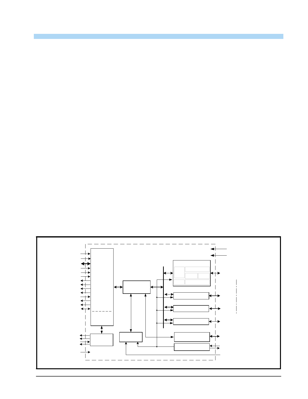
FIGURE 1. BLOCK DIAGRAM
CLK (33MHz)
RST#
AD[31:0]
C/BE[3:0]#
FRAME#
IRDY#
TRDY#
DEVSEL#
STOP#
INTA#
IDSEL
PERR#
SERR#
PAR
EECK
EEDI
EEDO
EECS
ENIR
PCI Local
Bus
Interface
Device
Configuration
Registers
Configuration
Space
Registers
EEPROM
Interface
16-bit
Timer/Counter
UART Channel 0
UART
Regs
BRG
64 Byte TX FIFO
TX & RX
IR
ENDEC
64 Byte RX FIFO
UART Channel 1
UART Channel 2
UART Channel 3
Multi-pur.pose
Inputs/Outputs
Crystal Osc/Buffer
5V VCC
GND
TX0, RX0, DTR0#,
DSR0#, RTS0#,
CTS0#, CD0#, RI0#
TX3, RX3, DTR3#,
DSR3#, RTS3#,
CTS3#, CD3#, RI3#
MPIO0- MPIO7
XTAL1
XTAL2
TMRCK
Exar Corporation 48720 Kato Road, Fremont CA, 94538 • (510) 668-7000 • FAX (510) 668-7017 • www.exar.com
1 page 
áç
REV. 1.3.0
Pin Description
XR17C154
5V PCI BUS QUAD UART
NAME
EECK
EECS
EEDI
EEDO
XTAL1
XTAL2
TMRCK
ENIR
TEST#
VCC
GND
NC
PIN #
116
115
114
113
110
109
69
70
111
4,19,34,45,64,
90,112,137
5,20,35,46,63,
89,136
47-54,
71,72,75-80,
91-98,
117-124
TYPE
DESCRIPTION
O Serial clock to EEPROM. An internal clock of CLK divide by 256 is used for
reading the vendor and sub-vendor ID during power up or reset. However, it
can be manually clocked thru the Configuration Register REGB.
O Chip select to a EEPROM device like 93C46. It is manually selectable thru the
Configuration Register REGB. Requires a pull-up 4.7K ohm resister for exter-
nal sensing of EEPROM during power up. See DAN112 for further details.
O Write data to EEPROM device. It is manually accessible thru the Configura-
tion Register REGB. The 154 auto-configuration register interface logic uses
the 16-bit format.
I Read data from EEPROM device. It is manually accessible thru the Configu-
ration Register REGB.
I Crystal or external clock input of up to 50MHz for data rate of 3.125Mbps at
5V.
O Crystal or buffered clock output.
I 16-bit timer/counter external clock input.
I Infrared mode enable (active high). This pin is sampled during power up, fol-
lowing a hardware reset (RST#) or soft-reset (register RESET). It can be used
to start up all 4 UARTs in the infrared mode. The sampled logic state is trans-
ferred to MCR bit-6 in the UART. Software can override this pin thereafter
and enable or disable it.
I Factory Test. Connect to VCC for normal operation.
PWR +5V (PCI Compliance). For 3.3V operation, see the XR17D154.
PWR Power supply common, ground.
No Connection. These pins are reserved and used by the octal PCI UART
XR17C158.
NOTE: Pin type: I=Input, O=Output, IO= Input/output, OD=Output Open Drain.
5
5 Page 
áç
REV. 1.3.0
XR17C154
5V PCI BUS QUAD UART
TABLE 3: DEVICE CONFIGURATION REGISTERS SHOWN IN BYTE ALIGNMENT
ADDRESS [A7:A0]
REGISTER
READ/WRITE COMMENT
RESET STATE
Ox080
INT0 [7:0] Read-only Interrupt [3:0], Reserved [7:4]
Bits 7-0 = 0x00
Ox081
INT1 [15:8] Read-only
Bits 7-0 = 0x00
Ox082
INT2 [23:16] Read-only [3:0], Reserved [7:4]
Bits 7-0 = 0x00
Ox083
INT3 [31:24] Reserved
Bits 7-0 = 0x00
Ox084
Ox085
Ox086
Ox087
TIMERCNTL
TIMER
TIMERLSB
TIMERMSB
Read/Write Timer Control
Reserved
Read/Write Timer LSB
Read/Write Timer MSB
Bits 7-0 = 0x00
Bits 7-0 = 0x00
Bits 7-0 = 0x00
Bits 7-0 = 0x00
Ox088
Ox089
Ox08A
Ox08B
8XMODE
REGA
RESET
SLEEP
Read/Write
Reserved
Write-only Self clear bits after executing Reset [3:0]
Read/Write Sleep mode [3:0]
Bits 7-0 = 0x00
Bits 7-0 = 0x00
Bits 7-0 = 0x00
Bits 7-0 = 0x00
Ox08C
Ox08D
Ox08E
Ox08F
DREV
DVID
REGB
MPIOINT
Read-only Device revision
Read-only Device identification
Write-only
Read/Write MPIO interrupt mask
Bits 7-0 = 0x02
Bits 7-0 = 0x24
Bits 7-0 = 0x00
Bits 7-0 = 0x00
Ox090
Ox091
Ox092
Ox093
MPIOLVL
MPIO3T
MPIOINV
MPIOSEL
Read/Write MPIO level control
Read/Write MPIO output control
Read/Write MPIO input polarity select
Read/Write MPIO select
Bits 7-0 = 0x00
Bits 7-0 = 0x00
Bits 7-0 = 0x00
Bits 7-0 = 0xFF
ADDRESS
0x080-083
0x084-087
0x088-08B
0x08C-08F
0x090-093
TABLE 4: DEVICE CONFIGURATION REGISTERS SHOWN IN DWORD ALIGNMENT
REGISTER
BYTE 3 [31:24] BYTE 2 [23:16] BYTE 1 [15:8]
BYTE 0 [7:0]
INTERRUPT (read-only)
INT3
INT2
INT1
INT0
TIMER (read/write)
TIMERMSB
TIMERLSB TIMER (reserved) TIMERCNTL
ANCILLARY1 (read/write)
SLEEP
RESET
REGA (reserved) 8XMODE
ANCILLARY2 (read-only)
MPIOINT
REGB
DVID
DREV
MPIO (read/write)
MPIOSEL
MPIOINV
MPIO3T
MPIOLVL
11
11 Page | ||
| Páginas | Total 30 Páginas | |
| PDF Descargar | [ Datasheet XR17C154.PDF ] | |
Hoja de datos destacado
| Número de pieza | Descripción | Fabricantes |
| XR17C152 | 5V PCI BUS DUAL UART | Exar Corporation |
| XR17C154 | 5V PCI BUS QUAD UART | Exar Corporation |
| XR17C158 | 5V PCI BUS OCTAL UART | Exar Corporation |
| Número de pieza | Descripción | Fabricantes |
| SLA6805M | High Voltage 3 phase Motor Driver IC. |
Sanken |
| SDC1742 | 12- and 14-Bit Hybrid Synchro / Resolver-to-Digital Converters. |
Analog Devices |
|
DataSheet.es es una pagina web que funciona como un repositorio de manuales o hoja de datos de muchos de los productos más populares, |
| DataSheet.es | 2020 | Privacy Policy | Contacto | Buscar |