|
|
|
PDF XRT73L00A Data sheet ( Hoja de datos )
| Número de pieza | XRT73L00A | |
| Descripción | E3/DS3/STS-1 LINE INTERFACE UNIT | |
| Fabricantes | Exar Corporation | |
| Logotipo | ||
Hay una vista previa y un enlace de descarga de XRT73L00A (archivo pdf) en la parte inferior de esta página. Total 30 Páginas | ||
|
No Preview Available !
áç
XRT73L00A
AUGUST 2002
E3/DS3/STS-1 LINE INTERFACE UNIT
REV. 2.0.1
GENERAL DESCRIPTION
The XRT73L00A DS3/E3/STS-1 Line Interface Unit is
an improved version of the XRT73L00 and consists of
a line transmitter and receiver integrated on a single
chip and is designed for DS3, E3 or SONET STS-1
applications.
XRT73L00A can be configured to support the E3
(34.368 Mbps), DS3 (44.736 Mbps) or the SONET
STS-1 (51.84 Mbps) rates.
In the transmit direction, the XRT73L00A encodes in-
put data to either B3ZS (for DS3/STS-1 applications)
or HDB3 (for E3 applications) format and converts the
data into the appropriate pulse shapes for transmis-
sion over coaxial cable via a 1:1 transformer.
In the receive direction the XRT73L00A performs
equalization on incoming signals, performs Clock Re-
covery, decodes data from either B3ZS or HDB3 for-
mat, converts the receive data into TTL/CMOS for-
mat, checks for LOS or LOL conditions and detects
and declares the occurrence of line code violations.
The XRT73L00A also contains a 4-Wire Microproces-
sor Serial Interface for accessing the on-chip Com-
mand registers.
FEATURES
• Incorporates an improved Timing Recovery circuit
and is pin and functional compatible to XRT73L00
• Meets E3/DS3/STS-1 Jitter Tolerance Require-
ments
• Full Loop-Back Capability
• Transmit and Receive Power Down Modes
• Full Redundancy Support
• Contains a 4-Wire Microprocessor Serial Interface
• Uses Minimum External components
• Single +3.3V Power Supply
• 5 V Tolerant pins
• -40°C to +85°C Operating Temperature Range
• Available in a 44 pin TQFP package
APPLICATIONS
• Interfaces to E3, DS3 or SONET STS-1 Networks
• CSU/DSU Equipment
• PCM Test Equipment
• Fiber Optic Terminals
• Multiplexers
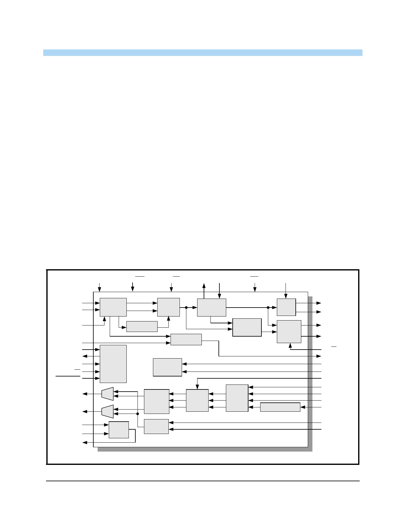
FIGURE 1. BLOCK DIAGRAM OF THE XRT73L00A
E3
S T S -1 /D S 3
Host/(HW )
RLOL EXCLK
ICT RCLKINV
R T IP
R R IN G
REQ DIS
LOSTHR
SDI
SDO /(LCV)
S C lk
CS
REGRESET
TTIP
T R IN G
M TIP
M RING
DMO
AGC/
Equalizer
Peak
Detector
Slicer
C lo c k
Recovery
LOS Detector
Serial
Processor
Interface
Loop MUX
Data
Recovery
Invert
HDB3/
B3ZS
Decoder
D e v ic e
M o n ito r
Pulse
Shaping
Tx
Control
HDB3/
B3ZS
Encoder
Transm it
Logic
Duty Cycle Adjust
RCLK1
L C V /(R C L K 2 )
RPOS
RNEG
D R /S R
RLOS
LLB
RLB
E N D E C D IS
TAOS
TPDATA
TNDATA
T C lk
TXLEV
TXOFF
Exar Corporation 48720 Kato Road, Fremont CA, 94538 • (510) 668-7000 • FAX (510) 668-7017 • www.exar.com
1 page 
áç
XRT73L00A
E3/DS3/STS-1 LINE INTERFACE UNIT
REV. 2.0.1
Figure 28. The Behavior of the RPOS and RCLK1 Output Signals While the XRT73L00A is Transmitting Single-
Rail Data to the Receiving Terminal Equipment ........................................................................... 38
4.0 Diagnostic Features of the XRT73L00A ................................................................... 38
4.1 THE ANALOG LOCAL LOOP-BACK MODE .............................................................................................. 38
Figure 29. The Analog Local Loop-Back in the XRT73L00A .......................................................................... 39
COMMAND REGISTER CR4 (ADDRESS = 0X04) ........................................................................................... 39
4.2 THE DIGITAL LOCAL LOOP-BACK MODE ............................................................................................... 39
Figure 30. The Digital Local Loop-Back path in the XRT73L00A ................................................................... 40
COMMAND REGISTER CR4 (ADDRESS = 0X04) ........................................................................................... 40
4.3 THE REMOTE LOOP-BACK MODE ......................................................................................................... 40
Figure 31. The Remote Loop-Back Path in the XRT73L00A .......................................................................... 41
4.4 TXOFF FEATURES .............................................................................................................................. 41
COMMAND REGISTER CR4 (ADDRESS = 0X04) ........................................................................................... 41
4.5 THE TRANSMIT DRIVE MONITOR FEATURES .......................................................................................... 41
COMMAND REGISTER CR1 (ADDRESS = 0X01) ........................................................................................... 41
Figure 32. The XRT73L00A Employing the Transmit Drive Monitor Features ............................................... 42
Figure 33. Two LIU’s, Each Monitoring the Transmit Output Signal of the Other LIU IC .............................. 43
4.6 THE TAOS (TRANSMIT ALL ONES) FEATURE ....................................................................................... 43
COMMAND REGISTER CR1 (ADDRESS = 0X01) ........................................................................................... 43
5.0 The Microprocessor Serial Interface ........................................................................ 44
5.1 DESCRIPTION OF THE COMMAND REGISTERS ........................................................................................ 44
TABLE 5: ADDRESSES AND BIT FORMATS OF XRT73L00A COMMAND REGISTERS .............................................. 44
DESCRIPTION OF BIT-FIELDS FOR EACH COMMAND REGISTER ..................................................................... 44
5.1.1 Command Register - CR0 ...................................................................................................... 44
5.1.2 Command Register - CR1 ...................................................................................................... 45
5.1.3 Command Register - CR2 ...................................................................................................... 46
5.1.4 Command Register - CR3 ...................................................................................................... 46
5.1.5 Command Register - CR4 ...................................................................................................... 46
5.2 OPERATING THE MICROPROCESSOR SERIAL INTERFACE. ...................................................................... 47
TABLE 6: LOOP-BACK MODES ........................................................................................................................... 47
Figure 34. Microprocessor Serial Interface Data Structure ............................................................................ 48
ORDERING INFORMATION ............................................................................................................................ 49
PACKAGE DIMENSIONS ................................................................................................. 49
REVISION HISTORY ..................................................................................................................................... 50
III
5 Page 
áç
PIN DESCRIPTION
PIN #
SYMBOL
30 LCV/(RCLK2)
31 RCLK1
32 RNEG
33 RPOS
34 ICT
XRT73L00A
E3/DS3/STS-1 LINE INTERFACE UNIT
REV. 2.0.1
TYPE
O
O
O
O
I
DESCRIPTION
Line Code Violation Indicator/Receive Clock Output pin 2:
The function of this pin depends upon whether the XRT73L00A is operating in
the HOST Mode, the Hardware Mode or User selection.
HOST Mode - Line Code Violation Indicator Output:
If the XRT73L00A is configured to operate in the HOST Mode, then this pin func-
tions as the LCV output pin by default. However, by using the on-chip Command
Registers, this pin can be configured to function as the second Receive Clock
signal output pin RCLK2.
Hardware Mode - Receive Clock Output pin 2:
This output pin is the Recovered Clock signal from the incoming line signal. The
receive section of the XRT73L00A outputs data via the RPOS and RNEG output
pins on the rising edge of this clock signal.
NOTE: If the XRT73L00A is operating in the HOST Mode and this pin is config-
ured to function as the additional Receive Clock signal output pin, then the
XRT73L00A can be configured to update the data on the RPOS and RNEG out-
put pins on the falling edge of this clock signal.
Receive Clock Output pin 1:
This output pin is the Recovered Clock signal from the incoming line signal. The
receive section of the XRT73L00A outputs data via the RPOS and RNEG output
pins on the rising edge of this clock signal.
NOTE: If the XRT73L00A is operating in the HOST Mode, the device can be con-
figured to update the data on the RPOS and RNEG output pins on the falling
edge of this clock signal.
Receive Negative Pulse Output:
This output pin pulses “High” whenever the XRT73L00A has received a Negative
Polarity pulse in the incoming line signal at the RTIP/RRING inputs.
NOTES:
1. If the B3ZS/HDB3 Decoder is enabled, the zero suppression patterns in
the incoming line signal (such as: "00V", "000V", "B0V", "B00V") are not
reflected at this output.
2. This output pin is inactive if the XRT73L00A has been configured to
operate in the Single-Rail Mode.
Receive Positive Pulse Output:
This output pin pulses “High” whenever the XRT73L00A has received a Positive
Polarity pulse in the incoming line signal at the RTIP/RRING inputs.
NOTE: If the B3ZS/HDB3 Decoder is enabled, the zero suppression patterns in
the incoming line signal (such as: "00V", "000V", "B0V", "B00V") are not
reflected at this output.
In-Circuit Test Input:
Setting this input pin “Low” causes all digital and analog outputs to go into a
high-impedance state in order to permit in-circuit testing. Set this pin “High” for
normal operation.
NOTE: This pin is internally pulled “High”.
8
11 Page | ||
| Páginas | Total 30 Páginas | |
| PDF Descargar | [ Datasheet XRT73L00A.PDF ] | |
Hoja de datos destacado
| Número de pieza | Descripción | Fabricantes |
| XRT73L00 | E3/DS3/STS-1 LINE INTERFACE UNIT | Exar Corporation |
| XRT73L00A | E3/DS3/STS-1 LINE INTERFACE UNIT | Exar Corporation |
| Número de pieza | Descripción | Fabricantes |
| SLA6805M | High Voltage 3 phase Motor Driver IC. |
Sanken |
| SDC1742 | 12- and 14-Bit Hybrid Synchro / Resolver-to-Digital Converters. |
Analog Devices |
|
DataSheet.es es una pagina web que funciona como un repositorio de manuales o hoja de datos de muchos de los productos más populares, |
| DataSheet.es | 2020 | Privacy Policy | Contacto | Buscar |