|
|
|
PDF XR16V2751 Data sheet ( Hoja de datos )
| Número de pieza | XR16V2751 | |
| Descripción | HIGH PERFORMANCE DUART | |
| Fabricantes | Exar Corporation | |
| Logotipo | ||
Hay una vista previa y un enlace de descarga de XR16V2751 (archivo pdf) en la parte inferior de esta página. Total 30 Páginas | ||
|
No Preview Available !
xrwww.DataSheet4U.com
PRELIMINARY
XR16V2751
HIGH PERFORMANCE DUART WITH 64-BYTE FIFO AND POWERSAVE FEATURE
JUNE 2006
GENERAL DESCRIPTION
FEATURES
REV. P1.0.0
The XR16V27511 (V2751) is a high performance dual
universal asynchronous receiver and transmitter
(UART) with 64 byte TX and RX FIFOs. The device
operates from 2.25 to 3.6 volts with 5 Volt tolerant
inputs and is pin-to-pin and software compatible to
Exar’s XR16L2751. The device includes 2 additional
capabilities over the XR16V2750: Intel and Motorola
data bus selection and a “PowerSave” mode to
further reduce sleep current to a minimum during
sleep mode. It supports the Exar’s enhanced features
of programmable FIFO trigger level and FIFO level
counters, automatic hardware (RTS/CTS) and
software flow control, automatic RS-485 half duplex
direction control output and a complete modem
interface. An internal loopback capability allows
system diagnostics. Independent programmable
fractional baud rate generators are provided in each
channel to select data rates up to 8 Mbps at 3.3 Volt
and 8X sampling clock. The V2751 is available in a
48-pin TQFP package.
NOTE: 1 Covered by U.S. Patent #5,649,122 and #5,949,787
APPLICATIONS
• Portable Appliances
• Telecommunication Network Routers
• Ethernet Network Routers
• Cellular Data Devices
• Factory Automation and Process Controls
• 2.25 to 3.6 Volt Operation
• 5 Volt Tolerant Inputs
• Pin-to-pin compatible to Exar’s XR16L2751 in the
48-TQFP package
• Two independent UART channels
■ Register set identical to 16L2751
■ Data rate of up to 8 Mbps at at 3.3 V, and
4 Mbps at 2.5 V with 8X sampling rate
■ Fractional Baud Rate Generator
■ Transmit and Receive FIFOs of 64 bytes
■ Programmable TX and RX FIFO Trigger Levels
■ Transmit and Receive FIFO Level Counters
■ Automatic Hardware (RTS/CTS) Flow Control
■ Selectable Auto RTS Flow Control Hysteresis
■ Automatic Software (Xon/Xoff) Flow Control
■ Automatic RS-485 Half-duplex Direction
Control Output via RTS#
■ Wireless Infrared (IrDA 1.0) Encoder/Decoder
■ Automatic sleep mode with wake-up interrupt
■ Full modem interface
• PowerSave Feature reduces sleep current to 15
µA
• Device Identification and Revision
• Crystal oscillator (up to 32MHz) or external clock
(upto 64MHz) input
• 48-TQFP package
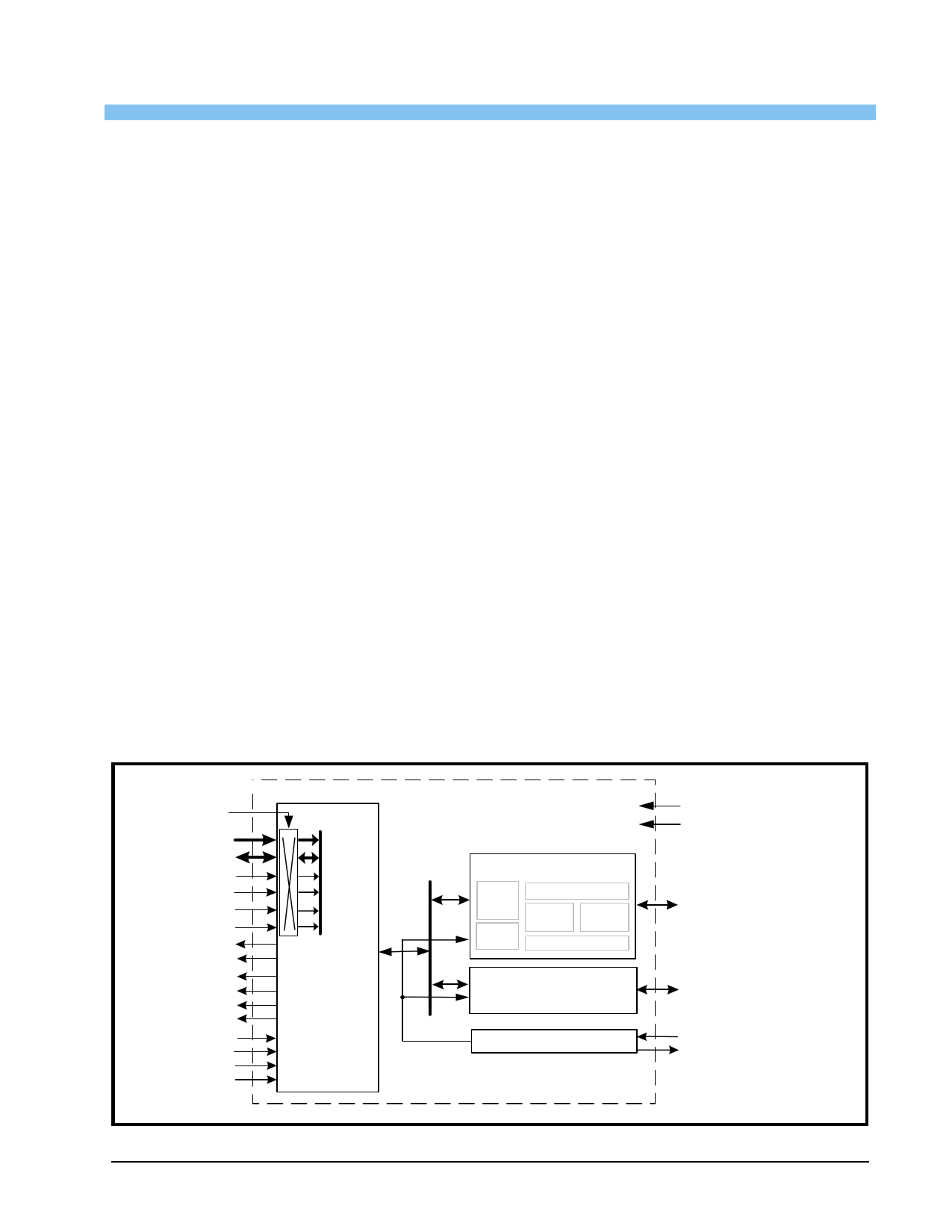
FIGURE 1. XR16V2751 BLOCK DIAGRAM
PwrSave
A2:A0
D7:D0
IOR# (VCC)
IOW# (R/W#)
CSA# (CS#)
CSB# (A3)
INTA (IRQ#)
INTB (logic 0)
TXRDYA#
TXRDYB#
RXRDYA#
RXRDYB#
Reset (Reset#)
16/68#
CLKSEL
HDCNTL#
Intel or
Motorola
Data Bus
Interface
*5 Volt Tolerant Inputs
(Except XTAL1)
UART Channel A
UART
Regs
BRG
64 Byte TX FIFO
TX & RX
IR
ENDEC
64 Byte RX FIFO
UART Channel B
(same as Channel A)
Crystal Osc/Buffer
2.25 to 3.6V VCC
GND
TXA, RXA, DTRA#,
DSRA#, RTSA#,
DTSA#, CDA#, RIA#,
OP2A#
TXB, RXB, DTRB#,
DSRB#, RTSB#,
CTSB#, CDB#, RIB#,
OP2B#
XTAL1
XTAL2
Exar Corporation 48720 Kato Road, Fremont CA, 94538 • (510) 668-7000 • FAX (510) 668-7017 • www.exar.com
1 page 
xr
REV. P1.0.0
PRELIMINARY
XR16V2751
HIGH PERFORMANCE DUART WITH 64-BYTE FIFO AND POWERSAVE FEATURE
Pin Description
NAME
OP2A#
TXB
RXB
RTSB#
CTSB#
DTRB#
DSRB#
CDB#
RIB#
OP2B#
48-TQFP
PIN #
32
8
4
22
23
35
20
16
21
9
TYPE
DESCRIPTION
O Output Port 2 Channel A - The output state is defined by the user and through the
software setting of MCR[3]. INTA is set to the active mode and OP2A# output LOW
when MCR[3] is set to a logic 1. INTA is set to the three state mode and OP2A# out-
put HIGH when MCR[3] is set to a logic 0. See MCR[3]. If INTA is used, this output
should not be used as a general output else it will disturb the INTA output functional-
ity.
O UART channel B Transmit Data or infrared encoder data. Standard transmit and
receive interface is enabled when MCR[6] = 0. In this mode, the TX signal will be
HIGH during reset or idle (no data). Infrared IrDA transmit and receive interface is
enabled when MCR[6] = 1. In the Infrared mode, the inactive state (no data) for the
Infrared encoder/decoder interface is LOW. If it is not used, leave it unconnected.
I UART channel B Receive Data or infrared receive data. Normal receive data input
must idle HIGH. The infrared receiver pulses typically idles at logic 0 but can be
inverted by software control prior going in to the decoder, see MCR[6] and FCTR[2].
If this pin is not used, tie it to VCC or pull it high via a 100k ohm resistor.
O UART channel B Request-to-Send (active low) or general purpose output. This port
must be asserted prior to using auto RTS flow control, see EFR[6], MCR[1],
FCTR[1:0], EMSR[5:4] and IER[6]. For auto RS485 half-duplex direction control, see
FCTR[3] and EMSR[3].
I UART channel B Clear-to-Send (active low) or general purpose input. It can be
used for auto CTS flow control, see EFR[7], and IER[7]. This input should be con-
nected to VCC when not used.
O UART channel B Data-Terminal-Ready (active low) or general purpose output. If it is
not used, leave it unconnected.
I UART channel B Data-Set-Ready (active low) or general purpose input. This input
should be connected to VCC when not used. This input has no effect on the UART.
I UART channel B Carrier-Detect (active low) or general purpose input. This input
should be connected to VCC when not used. This input has no effect on the UART.
I UART channel B Ring-Indicator (active low) or general purpose input. This input
should be connected to VCC when not used. This input has no effect on the UART.
O Output Port 2 Channel B - The output state is defined by the user and through the
software setting of MCR[3]. INTB is set to the active mode and OP2B# output LOW
when MCR[3] is set to a logic 1. INTB is set to the three state mode and OP2B# out-
put HIGH when MCR[3] is set to a logic 0. See MCR[3]. If INTB is used, this output
should not be used as a general output else it will disturb the INTB output functional-
ity.
ANCILLARY SIGNALS
XTAL1
13
XTAL2
14
I Crystal or external clock input. Caution: this input is not 5V tolerant.
O Crystal or buffered clock output.
PwrSave
12
I PowerSave (active high). This feature isolates the 2751’s data bus interface from the
host preventing other bus activities that cause higher power drain during sleep mode.
See Sleep Mode with Auto Wake-up and PowerSave Feature section for details.
5
5 Page 
xr
REV. P1.0.0
PRELIMINARY
XR16V2751
HIGH PERFORMANCE DUART WITH 64-BYTE FIFO AND POWERSAVE FEATURE
2.9 Crystal Oscillator or External Clock Input
The V2751 includes an on-chip oscillator (XTAL1 and XTAL2) to produce a clock for both UART sections in the
device. The CPU data bus does not require this clock for bus operation. The crystal oscillator provides a
system clock to the Baud Rate Generators (BRG) section found in each of the UART. XTAL1 is the input to the
oscillator or external clock buffer input with XTAL2 pin being the output. Please note that the input XTAL1 is not
5V tolerant and so the maximum at the pin should be VCC. For programming details, see ““Section 2.10,
Programmable Baud Rate Generator with Fractional Divisor” on page 11.”
FIGURE 4. TYPICAL OSCILLATOR CONNECTIONS
XTAL1
XTAL2
R1
0-120 Ω
R2 (Optional)
500 ΚΩ− 1 ΜΩ
C1
22-47 pF
Y1
1.8432 MHz
to
24 MHz
C2
22-47 pF
The on-chip oscillator is designed to use an industry standard microprocessor crystal (parallel resonant,
fundamental frequency with 10-22 pF capacitance load, ESR of 20-120 ohms and 100 ppm frequency
tolerance) connected externally between the XTAL1 and XTAL2 pins (see Figure 4). The programmable Baud
Rate Generator is capable of operating with a crystal oscillator frequency of up to 24 MHz. However, with an
external clock input on XTAL1 pin, it can extend its operation up to 64 MHz (8 Mbps serial data rate) at 3.3V
with an 8X sampling rate. For further reading on the oscillator circuit please see the Application Note DAN108
on the EXAR web site at http://www.exar.com.
2.10 Programmable Baud Rate Generator with Fractional Divisor
Each UART has its own Baud Rate Generator (BRG) with a prescaler for the transmitter and receiver. The
prescaler is controlled by a software bit in the MCR register. The MCR register bit-7 sets the prescaler to divide
the input crystal or external clock by 1 or 4. The output of the prescaler clocks to the BRG. The BRG further
divides this clock by a programmable divisor between 1 and (216 - 0.0625) in increments of 0.0625 (1/16) to
obtain a 16X or 8X sampling clock of the serial data rate. The sampling clock is used by the transmitter for data
bit shifting and receiver for data sampling. The BRG divisor (DLL, DLM and DLD registers) defaults to the value
of ’1’ (DLL = 0x01, DLM = 0x00 and DLD = 0x00) upon reset. Therefore, the BRG must be programmed during
initialization to the operating data rate. The DLL and DLM registers provide the integer part of the divisor and
the DLD register provides the fractional part of the dvisior. Only the four lower bits of the DLD are implemented
and they are used to select a value from 0 (for setting 0000) to 0.9375 or 15/16 (for setting 1111). Programming
the Baud Rate Generator Registers DLL, DLM and DLD provides the capability for selecting the operating data
rate. Table 6 shows the standard data rates available with a 24MHz crystal or external clock at 16X clock rate.
If the pre-scaler is used (MCR bit-7 = 1), the output data rate will be 4 times less than that shown in Table 6. At
8X sampling rate, these data rates would double. Also, when using 8X sampling mode, please note that the bit-
11
11 Page | ||
| Páginas | Total 30 Páginas | |
| PDF Descargar | [ Datasheet XR16V2751.PDF ] | |
Hoja de datos destacado
| Número de pieza | Descripción | Fabricantes |
| XR16V2750 | HIGH PERFORMANCE DUART | Exar Corporation |
| XR16V2751 | HIGH PERFORMANCE DUART | Exar Corporation |
| XR16V2752 | HIGH PERFORMANCE DUART | Exar Corporation |
| Número de pieza | Descripción | Fabricantes |
| SLA6805M | High Voltage 3 phase Motor Driver IC. |
Sanken |
| SDC1742 | 12- and 14-Bit Hybrid Synchro / Resolver-to-Digital Converters. |
Analog Devices |
|
DataSheet.es es una pagina web que funciona como un repositorio de manuales o hoja de datos de muchos de los productos más populares, |
| DataSheet.es | 2020 | Privacy Policy | Contacto | Buscar |