|
|
|
PDF XR16L651 Data sheet ( Hoja de datos )
| Número de pieza | XR16L651 | |
| Descripción | 2.25V TO 5.5V UART | |
| Fabricantes | Exar Corporation | |
| Logotipo | ||
Hay una vista previa y un enlace de descarga de XR16L651 (archivo pdf) en la parte inferior de esta página. Total 56 Páginas | ||
|
No Preview Available !
áçwww.DataSheet4U.com
JANUARY 2004
GENERAL DESCRIPTION
The XR16L6511 (651) is a 2.25 to 5.5 volt Universal
Asynchronous Receiver and Transmitter (UART) with
5 volt tolerant inputs. This device supports Intel and
Motorola data bus interfaces and is software
compatible to industry standard 16C450, 16C550,
ST16C580 and ST16C650A UARTs.
The 651 has 32 bytes of TX and RX FIFOs and is
capable of operating up to serial data rates of 3.125
Mbps at 5 volt supply voltage. The internal registers
include the 16C550 register set plus Exar’s enhanced
registers for additional features to support today’s
highly demanding data communication needs. The
enhanced features include automatic hardware and
software flow control, selectable TX and RX trigger
levels, and wireless infrared (IrDA) encoder/decoder.
The device provides a new capability to give user the
ability to program the wireless infrared encoder
output pulse width, hence reducing the power
consumption of a handheld unit.
The XR16L651 device comes in a small 7x7x1mm
48-pin TQFP package in both the commercial and
industrial temperature ranges.
NOTE: 1 Covered by US patents #5,649,122.
XR16L651
2.25V TO 5.5V UART WITH 32-BYTE FIFO
FEATURES
REV. 1.3.0
Added feature in devices with top mark date code of
"C2 YYWW" and newer:
s 0 ns address hold time
• 2.25 to 5.5 Volt Operation w/ 5 Volt Tolerant Inputs
• ST16C450/550/580/650A Software Compatible
• Intel, Motorola or PC Mode 8-bit Bus Interface
• Up to 3.125 Mbps Data Rate at 5 Volt Operation
• 32-byte Transmit and Receive FIFOs
• Automatic RS485 Half-Duplex Control Output
• Automatic Hardware (RTS/CTS) Flow Control
• Hardware Flow Control Hysteresis
• Automatic Software (Xon/Xoff) Flow Control
• Infrared (IrDA) Encoder/Decoder Enable Input
• Programmable Infrared Encoder Pulse Width
• Sleep Mode with Wake-up Indicator via interrupt
APPLICATIONS
• Battery Operated Electronics
• Internet Appliances
• Handheld Terminal
• Personal Digital Assistants
• Cellular Phones DataPort
• Wireless Infrared Data Communications Systems
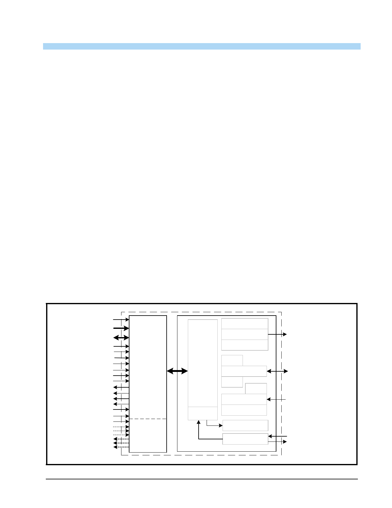
FIGURE 1. BLOCK DIAGRAM
RESET
A2:A0
D7:D0
IOR#
IOR
IOW#/R/W#
IOW
CS2#
CS1
CS0
INT
TXRDY#
RDRDY#
DDIS#
ENIR
IM#
PCMODE#
S1
S2
S3
IRQA
IRQB
IRQC
Intel,
Motorola
or PC
Data Bus
Interface
PC Mode:
COM 1 to 4
Decode Logic
UART
Configuration
Regs
BRG
Prescaler
32 Byte TX FIFO
Transmitter
Infrared Encoder and
Pulse Width Control
CTS Flow
Control
Modem Control Signals
RTS Flow
Control
Infrared
Decoder
Receiver with Auto
Software Flow Control
32 Byte RX FIFO
Baud Rate Generator
Crystal Osc/Buffer
TX
DTR#, DSR#,
RTS#, CTS#,
CD#, RI#
RX
XTAL1/CLK
XTAL2
Exar Corporation 48720 Kato Road, Fremont CA, 94538 • (510) 668-7000 • FAX (510) 668-7017 • www.exar.com
1 page 
áç
REV. 1.3.0
XR16L651
2.25V TO 5.5V UART WITH 32-BYTE FIFO
NAME
PIN #
TYPE
DESCRIPTION
AEN#
24 I Address Enable input (active low)
When AEN# transition to logic 0, it decodes and validates COM 1-4 ports
address per S1, S2 and S3 inputs.
S1 21 I Select 1 to 3
S2 5
These are the standard PC COM 1-4 ports and IRQ selection inputs. See
S3 31
Table 1 and Table 3 for details. The S1 pin has an internal 100kΩ pull-up
resistor.
IRQA
IRQB
IRQC
30 O Interrupt Request A, B and C Outputs (active high, tri-state)
29 These are the interrupt outputs associated with COM 1-4 to be connected to
23 the host data bus. See interrupt section for details. The Interrupt Requests A,
B or C functions as IRQx to the PC bus. IRQx is enabled by setting MCR bit-3
to logic 1 and the desired interrupt(s) in the interrupt enable register (IER).
LPT1#
12 O Line Printer Port-1 Decode Logic Output (active low)
This pin functions as the PC standard LPT-1 printer port address decode logic
output, see Table 1. The baud rate generator clock output, BAUDOUT#, is
internally connected to the RCLK input in the PC mode.
LPT2#
22 O Line Printer Port-2 Decode Logic Output (active low)
This pin functions as the PC standard LPT-2 printer port address decode logic
output, see Table 1.
MODEM OR SERIAL I/O INTERFACE
TX 8 O Transmit Data or wireless infrared transmit data
This output is active low in normal standard serial interface operation (RS-
232, RS-422 or RS-485) and active high in the infrared mode. Infrared mode
can be enabled by connecting pin ENIR to VCC or through software setting
after power up.
RX 7 I Receive Data or wireless infrared receive data
Normal received data input idles at logic 1 condition and logic 0 in the infrared
mode. The wireless infrared pulses are applied to the decoder. This input
must be connected to its idle logic state in either normal, logic 1, or infrared
mode, logic 0, else the receiver may report “receive break” and/or “error” con-
dition(s).
RTS#
32 O Request to Send or general purpose output (active low)
This port may be used for one of two functions:
1) automatic hardware flow control, see EFR bit-6, MCR bit-1and IER bit-6.
2) RS485 half-duplex direction control, see XFR bits 2 and 5.
RTS# output must be asserted before auto RTS flow control can start.
CTS#
39 I Clear to Send or general purpose input (active low)
If used for automatic hardware flow control, data transmission will be stopped
when this pin is de-asserted and will resume when this pin is asserted again.
See EFR bit-7 and IER bit-7.
DTR#
33 O Data Terminal Ready or general purpose output (active low)
DSR#
40 I Data Set Ready input or general purpose input (active low)
CD#
41 I Carrier Detect input or general purpose input (active low)
RI# 42 I Ring Indicator input or general purpose input (active low)
ANCILLARY SIGNALS
5
5 Page 
áç
REV. 1.3.0
XR16L651
2.25V TO 5.5V UART WITH 32-BYTE FIFO
2.2 5-Volt Tolerant Inputs
The 651 can acccept up to 5V inputs even when operating at 3.3V or 2.5V. But note that if the 651 is operating
at 2.5V, its VOH may not be high enough to meet the requirements of the VIH of a CPU or a serial transceiver
that is operating at 5V. Caution: XTAL1 is not 5 volt tolerant.
2.3 Device Reset
The RESET input resets the internal registers and the serial interface outputs to their default state (see
Figure 13). An active high pulse of longer than 40 ns duration will be required to activate the reset function in
the device.
2.4 Device Identification and Revision
The XR16L651 provides a Device Identification code and a Device Revision code to distinguish the part from
other devices and revisions. To read the identification code from the part, it is required to set the baud rate
generator registers DLL and DLM both to 0x00. Now reading the content of the DLM will provide 0x04 for the
XR16L651 and reading the content of DLL will provide the revision of the part; for example, a reading of 0x01
means revision A.
2.5 DMA Mode
The device does not support direct memory access. The DMA Mode (a legacy term) in this document does not
mean “direct memory access” but refers to data block transfer operation. The DMA mode affects the state of
the RXRDY# and TXRDY# output pins. The transmit and receive FIFO trigger levels provide additional
flexibility to the user for block mode operation. The LSR bits 5-6 provide an indication when the transmitter is
empty or has an empty location(s) for more data. The user can optionally operate the transmit and receive
FIFO in the DMA mode (FCR bit-3=1). When the transmit and receive FIFO are enabled and the DMA mode is
disabled (FCR bit-3 = 0), the 651 is placed in single-character mode for data transmit or receive operation.
When DMA mode is enabled (FCR bit-3 = 1), the user takes advantage of block mode operation by loading or
unloading the FIFO in a block sequence determined by the programmed trigger level. In this mode, the 651
sets the TXRDY# pin when the transmit FIFO becomes full, and sets the RXRDY# pin when the receive FIFO
becomes empty. The following table shows their behavior. Also see Figures 26 through 31.
TABLE 2: TXRDY# AND RXRDY# OUTPUTS IN FIFO AND DMA MODE
PINS
FCR BIT-0=0
(FIFO DISABLED)
FCR BIT-0=1 (FIFO ENABLED)
FCR BIT-3 = 0
(DMA MODE DISABLED)
FCR BIT-3 = 1
(DMA MODE ENABLED)
RXRDY# 0 = 1 byte.
1 = no data.
0 = at least 1 byte in FIFO
1 = FIFO empty.
1 to 0 transition when FIFO reaches the trigger
level, or timeout occurs.
0 to 1 transition when FIFO empties.
TXRDY# 0 = THR empty.
1 = byte in THR.
0 = FIFO empty.
1 = at least 1 byte in FIFO.
0 = FIFO has at least 1 empty location.
1 = FIFO is full.
11
11 Page | ||
| Páginas | Total 56 Páginas | |
| PDF Descargar | [ Datasheet XR16L651.PDF ] | |
Hoja de datos destacado
| Número de pieza | Descripción | Fabricantes |
| XR16L651 | 2.25V TO 5.5V UART | Exar Corporation |
| Número de pieza | Descripción | Fabricantes |
| SLA6805M | High Voltage 3 phase Motor Driver IC. |
Sanken |
| SDC1742 | 12- and 14-Bit Hybrid Synchro / Resolver-to-Digital Converters. |
Analog Devices |
|
DataSheet.es es una pagina web que funciona como un repositorio de manuales o hoja de datos de muchos de los productos más populares, |
| DataSheet.es | 2020 | Privacy Policy | Contacto | Buscar |