|
|
|
PDF XR16L2750 Data sheet ( Hoja de datos )
| Número de pieza | XR16L2750 | |
| Descripción | 2.25V TO 5.5V DUART | |
| Fabricantes | Exar Corporation | |
| Logotipo | ||
Hay una vista previa y un enlace de descarga de XR16L2750 (archivo pdf) en la parte inferior de esta página. Total 49 Páginas | ||
|
No Preview Available !
áçwww.DataSheet4U.com
XR16L2750
2.25V TO 5.5V DUART WITH 64-BYTE FIFO
SEPTEMBER 2002
REV. 1.0.0
GENERAL DESCRIPTION
The XR16L27501 (2750) is a low voltage dual
universal asynchronous receiver and transmitter
(UART) with 5 Volt tolerant inputs. The device
operates from 2.25 to 5.5 Volt supply range and is
pin-to-pin compatible to Exar’s ST16C2550 and
XR16C2850 except the 48-TQFP package. The 2750
register set is compatible to the ST16C2550 and the
XR16C2850 enhanced features. It supports the
Exar’s enhanced features of 64 bytes of TX and RX
FIFOs, programmable FIFO trigger level and FIFO
level counters, automatic hardware (RTS/CTS) and
software flow control, automatic RS-485 half duplex
direction control output and a complete modem
interface. Onboard registers provide the user with
operational status and data error flags. An internal
loopback capability allows system diagnostics.
Independent programmable baud rate generators are
provided in each channel to select data rates up to
6.25 Mbps at 5 Volt and 8X sampling clock. The 2750
is available in 48-pin TQFP and 44-pin PLCC
packages.
NOTE: 1 Covered by U.S. Patent #5,649,122 and #5,832,205
APPLICATIONS
• Portable Appliances
• Telecommunication Network Routers
• Ethernet Network Routers
• Cellular Data Devices
• Factory Automation and Process Controls
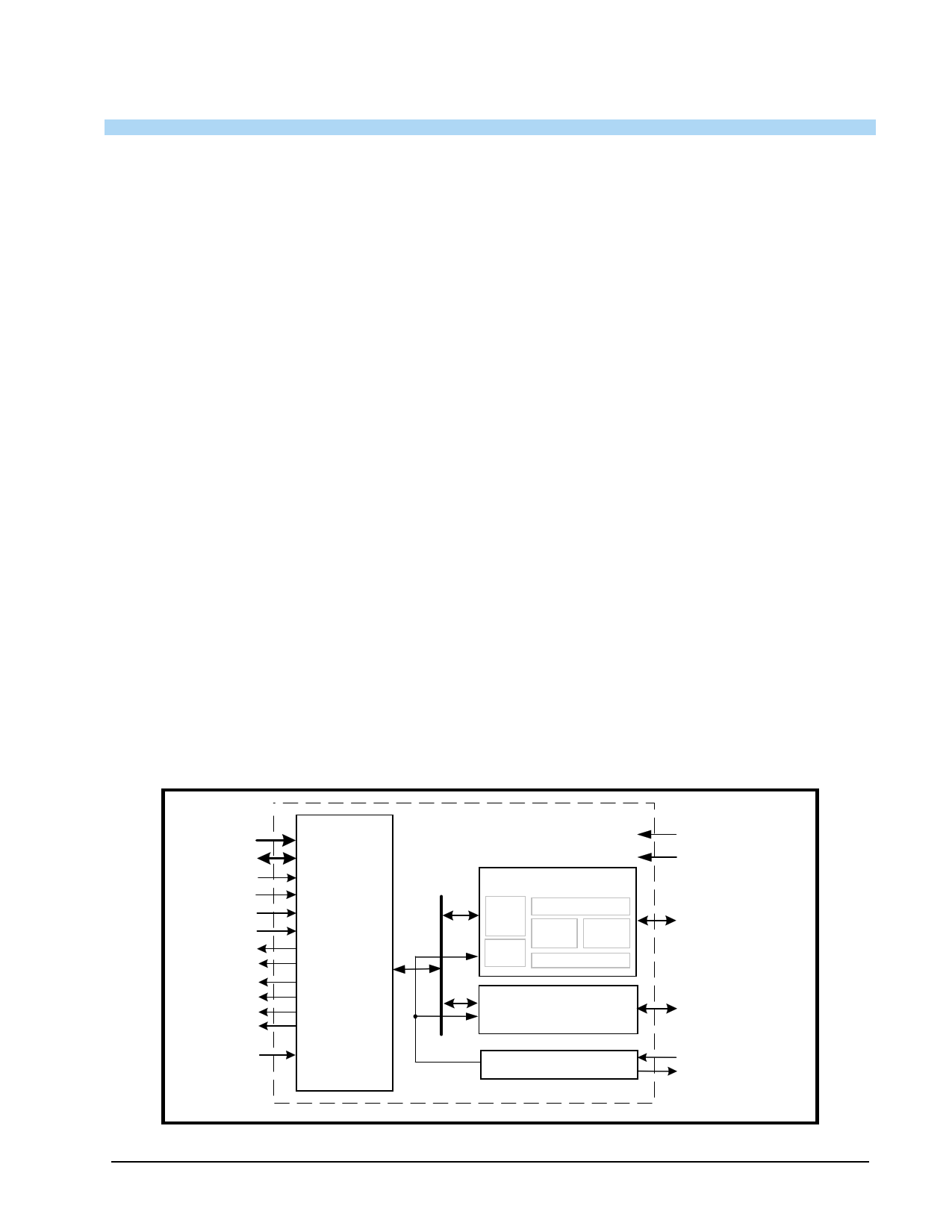
FIGURE 1. XR16L2750 BLOCK DIAGRAM
FEATURES
• 2.25 to 5.5 Volt Operation
• 5 Volt Tolerant Inputs
• Pin-to-pin compatible to Exar’s ST16C2550 and
TI’s TL16C752B on the 48-TQFP package
• Pin alike XR16C2850 48-TQFP package but
without CLK8/16, CLKSEL and HDCNTL inputs
• Two independent UART channels
s Reg set compatible to 16C2550 and 16C2850
s Up to 6.25 Mbps at 5 Volt, 4 Mbps at 3.3 Volt,
and 3 Mbps at 2.5 Volt with 8X sampling rate
s Transmit and Receive FIFOs of 64 bytes
s Programmable TX and RX FIFO Trigger Levels
s Transmit and Receive FIFO Level Counters
s Automatic Hardware (RTS/CTS) Flow Control
s Selectable Auto RTS Flow Control Hysteresis
s Automatic Software (Xon/Xoff) Flow Control
s Automatic RS-485 Half-duplex Direction
Control Output via RTS#
s Wireless Infrared (IrDA 1.0) Encoder/Decoder
s Automatic sleep mode
s Full modem interface
• Device Identification and Revision
• Crystal oscillator or external clock input
• Industrial and commercial temperature ranges
• 48-TQFP and 44-PLCC packages
A2:A0
D7:D0
IOR#
IOW#
CSA#
CSB#
INTA
INTB
TXRDYA#
TXRDYB#
RXRDYA#
RXRDYB#
Reset
8-bit Data
Bus
Interface
* 5 Volt Tolerant Inputs
UART Channel A
UART
Regs
BRG
64 Byte TX FIFO
TX & RX
IR
ENDEC
UART Channel B
(same as Channel A)
Crystal Osc/Buffer
2.25 to 5.5 Volt VCC
GND
TXA, RXA, DTRA#,
DSRA#, RTSA#,
DTSA#, CDA#, RIA#,
OP2A#
TXB, RXB, DTRB#,
DSRB#, RTSB#,
CTSB#, CDB#, RIB#,
OP2B#
XTAL1
XTAL2
2750BLK
Exar Corporation 48720 Kato Road, Fremont CA, 94538 • (510) 668-7000 • FAX (510) 668-7017 • www.exar.com
1 page 
XR16L2750
2.25V TO 5.5V DUART WITH 64-BYTE FIFO
REV. 1.0.0
áç
Pin Description
NAME
RXB
RTSB#
CTSB#
DTRB#
DSRB#
CDB#
RIB#
OP2B#
44-PLCC
PIN #
10
27
28
38
25
21
26
15
48-TQFP
PIN #
4
22
23
35
20
16
21
9
TYPE
DESCRIPTION
I UART channel B Receive Data or infrared receive data. Normal receive
data input must idle at logic 1 condition. The infrared receiver pulses
typically idles at logic 0 but can be inverted by software control prior
going in to the decoder, see MCR[6] and FCTR[2]. If this pin is not
used, tie it to VCC or pull it high via a 100k ohm resistor.
O UART channel B Request-to-Send (active low) or general purpose out-
put. This port must be asserted prior to using auto RTS flow control,
see EFR[6], MCR[1], FCTR[1:0], EMSR[5:4] and IER[6]. For auto
RS485 half-duplex direction control, see FCTR[3] and EMSR[3].
I UART channel B Clear-to-Send (active low) or general purpose input.
It can be used for auto CTS flow control, see EFR[7], and IER[7]. This
input should be connected to VCC when not used.
O UART channel B Data-Terminal-Ready (active low) or general purpose
output. If it is not used, leave it unconnected.
I UART channel B Data-Set-Ready (active low) or general purpose input.
This input should be connected to VCC when not used. This input has
no effect on the UART.
I UART channel B Carrier-Detect (active low) or general purpose input.
This input should be connected to VCC when not used. This input has
no effect on the UART.
I UART channel B Ring-Indicator (active low) or general purpose input.
This input should be connected to VCC when not used. This input has
no effect on the UART.
O Output Port 2 Channel B - The output state is defined by the user and
through the software setting of MCR[3]. INTB is set to the active mode
and OP2B# output to a logic 0 when MCR[3] is set to a logic 1. INTB is
set to the three state mode and OP2B# to a logic 1 when MCR[3] is set
to a logic 0. See MCR[3]. This output should not be used as a general
output else it will disturb the INTB output functionality.
ANCILLARY SIGNALS
XTAL1
18
XTAL2
19
RESET
39
VCC
GND
N.C.
44
22
none
13
14
36
42
17
12, 24, 25,
37
I Crystal or external clock input. Caution: this input is not 5V tolerant.
O Crystal or buffered clock output.
I Reset (active high) - A longer than 40 ns logic 1 pulse on this pin will
reset the internal registers and all outputs. The UART transmitter output
will be held at logic 1, the receiver input will be ignored and outputs are
reset during reset period (see External Reset Conditions).
Pwr 2.25V to 5.5V power supply. All input pins, except XTAL1, are 5V toler-
ant.
Pwr Power supply common, ground.
No Connection. These pins are open, but typically, should be con-
nected to GND for good design practice.
Pin type: I=Input, O=Output, I/O= Input/output, OD=Output Open Drain.
5
5 Page 
XR16L2750
2.25V TO 5.5V DUART WITH 64-BYTE FIFO
REV. 1.0.0
áç
sampling clock rate mode (EMSR bit-7=0) to double the operating data rate. When using a non-standard data
rate crystal or external clock, the divisor value can be calculated for DLL/DLM with the following equation.
divisor (decimal) = (XTAL1 clock frequency / prescaler) / (serial data rate x 16), with 16XMode [EMSR bit-7] = 1
divisor (decimal) = (XTAL1 clock frequency / prescaler) / (serial data rate x 8), with 16XMode [EMSR bit-7] = 0
TABLE 5: TYPICAL DATA RATES WITH A 14.7456 MHZ CRYSTAL OR EXTERNAL CLOCK
OUTPUT Data Rate OUTPUT Data Rate
MCR Bit-7=1
MCR Bit-7=0 DIVISOR FOR 16x DIVISOR FOR 16x
Clock (Decimal) Clock (HEX)
(DEFAULT)
DLM
PROGRAM
VALUE (HEX)
DLL
PROGRAM
VALUE (HEX)
DATA RATE
ERROR (%)
100 400 2304 900 09 00 0
600
2400
384 180 01 80 0
1200
4800 192 C0 00 C0 0
2400 9600 96 60 00 60 0
4800
19.2k
48
30 00 30 0
9600
38.4k
24
18 00 18 0
19.2k
76.8k
12
0C 00 0C 0
38.4k
153.6k
6
06 00 06 0
57.6k
230.4k
4
04 00 04 0
115.2k
460.8k
2
02 00 02 0
230.4k
921.6k
1
01 00 01 0
2.11 Transmitter
The transmitter section comprises of an 8-bit Transmit Shift Register (TSR) and 64 bytes of FIFO which
includes a byte-wide Transmit Holding Register (THR). TSR shifts out every data bit with the 16X/8X internal
clock. A bit time is 16 (8) clock periods (see EMSR bit-7). The transmitter sends the start-bit followed by the
number of data bits, inserts the proper parity-bit if enabled, and adds the stop-bit(s). The status of the FIFO
and TSR are reported in the Line Status Register (LSR bit-5 and bit-6).
2.11.1 Transmit Holding Register (THR) - Write Only
The transmit holding register is an 8-bit register providing a data interface to the host processor. The host
writes transmit data byte to the THR to be converted into a serial data stream including start-bit, data bits,
parity-bit and stop-bit(s). The least-significant-bit (Bit-0) becomes first data bit to go out. The THR is the input
register to the transmit FIFO of 64 bytes when FIFO operation is enabled by FCR bit-0. Every time a write
operation is made to the THR, the FIFO data pointer is automatically bumped to the next sequential data
location.
2.11.2 Transmitter Operation in non-FIFO Mode
The host loads transmit data to THR one character at a time. The THR empty flag (LSR bit-5) is set when the
data byte is transferred to TSR. THR flag can generate a transmit empty interrupt (ISR bit-1) when it is enabled
by IER bit-1. The TSR flag (LSR bit-6) is set when TSR becomes completely empty.
11
11 Page | ||
| Páginas | Total 49 Páginas | |
| PDF Descargar | [ Datasheet XR16L2750.PDF ] | |
Hoja de datos destacado
| Número de pieza | Descripción | Fabricantes |
| XR16L2750 | 2.25V TO 5.5V DUART | Exar Corporation |
| XR16L2751 | 2.25V TO 5.5V DUART WITH 64-BYTE FIFO AND POWERSAVE | Exar Corporation |
| XR16L2752 | 2.25V TO 5.5V DUART | Exar Corporation |
| Número de pieza | Descripción | Fabricantes |
| SLA6805M | High Voltage 3 phase Motor Driver IC. |
Sanken |
| SDC1742 | 12- and 14-Bit Hybrid Synchro / Resolver-to-Digital Converters. |
Analog Devices |
|
DataSheet.es es una pagina web que funciona como un repositorio de manuales o hoja de datos de muchos de los productos más populares, |
| DataSheet.es | 2020 | Privacy Policy | Contacto | Buscar |