|
|
|
PDF 33291L Data sheet ( Hoja de datos )
| Número de pieza | 33291L | |
| Descripción | Eight-Output Switch | |
| Fabricantes | Freescale Semiconductor | |
| Logotipo | ||
Hay una vista previa y un enlace de descarga de 33291L (archivo pdf) en la parte inferior de esta página. Total 25 Páginas | ||
|
No Preview Available !
www.DFaretaeSshceeatl4eUS.ceommiconductor
Technical Data
Eight-Output Switch with Serial
Peripheral Interface I/O
Document Number: MC33291L
Rev. 4.0, 11/2006
33291L
The 33291L device is an eight-output, low-side power switch with 8-
bit serial input control. The 33291L is a versatile circuit designed for
automotive applications, but is well suited for other environments. The
33291L incorporates SMARTMOS technology, with CMOS logic,
bipolar/MOS analog circuitry, and DMOS power MOSFETs. The
33291L interfaces directly with a microcontroller to control various
inductive or incandescent loads.
The circuit’s innovative monitoring and protection features include
very low standby current, SPI cascade fault reporting capability,
internal 53 V clamp on each output, output-specific diagnostics, and
independent shutdown of outputs.
The device is parametrically specified over an ambient temperature
range of -40°C ≤ TA ≤ 125°C and 9.0 V ≤ VPWR ≤ 16 V supply.
Features
• Designed to Operate Over Wide Supply Voltages of 5.5 V to 26.5 V
• Interfaces to Microprocessor Using 8-Bit SPI I/O Protocol up to 3.0
MHz
• 1.0 A Peak Current Outputs with Maximum RDS(ON) of 1.6 Ω at TJ -
150°C
• Outputs Current-Limited to Accommodate In-Rush Currents
Associated with Switching Incandescent Loads
• Output Voltages Clamped to 53 V During Inductive Switching
• Maximum Sleep Current (IPWR) of 25 µA
• Maximum of 4.0 mA IDD During Operation
• Pb-Free Packaging Designated by Suffix Code EG
LOW-SIDE SWITCH
DW SUFFIX
EG SUFFIX (PB-FREE)
98ASB42344B
24-PIN SOICW
ORDERING INFORMATION
Device
Temperature
Range (TA)
Package
MC33291LDW/R2
-40°C to 125°C
MCZ33291LEG/R2
24 SOICW
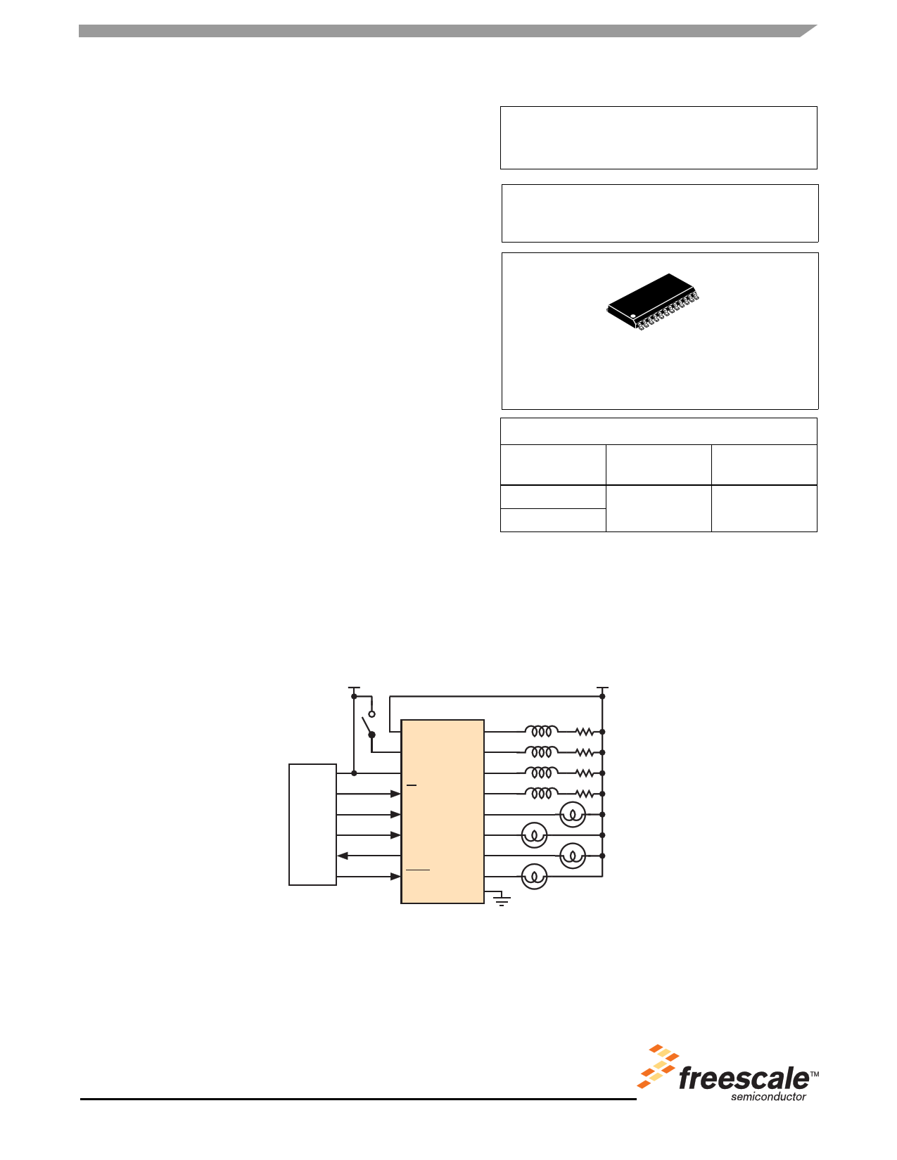
VDD
MCU
33291L
VPWR OP 0
SFPD OP 1
VDD OP 2
CS
SCLK
SI
SO
RESET
OP 3
OP 4
OP 5
OP 6
OP 7
GND
V PWR
Figure 1. 33291L Simplified Application Schematic
Freescale Semiconductor, Inc. reserves the right to change the detail specifications, as
may be required, to permit improvements in the design of its products.
© Freescale Semiconductor, Inc., 2007. All rights reserved.
1 page 
ELECTRICAL CHARACTERISTICS
MAXIMUM RATINGS
Table 3. Maximum Ratings (continued)
All voltages are with respect to ground unless otherwise noted. Exceeding these ratings may cause a malfunction or
permanent damage to the device.
Rating
Peak Package Reflow Temperature During Reflow (10), (11)
Thermal Resistance
All Outputs ON(12)
Single Output ON(13)
Symbol
TPPRT
RθJA
Value
Note 11.
60
45
Unit
°C
°C/W
Notes
10. Pin soldering temperature limit is for 10 seconds maximum duration. Not designed for immersion soldering. Exceeding these limits may
cause malfunction or permanent damage to the device.
11. Freescale’s Package Reflow capability meets Pb-free requirements for JEDEC standard J-STD-020C. For Peak Package Reflow
Temperature and Moisture Sensitivity Levels (MSL),
Go to www.freescale.com, search by part number [e.g. remove prefixes/suffixes and enter the core ID to view all orderable parts. (i.e.
MC33xxxD enter 33xxx), and review parametrics.
12. Junction temperature is a function of die size, on-chip power dissipation, package thermal resistance, mounting site (board)
temperature, ambient temperature, air flow, power dissipation of other components on the board, and board thermal resistance.
13. Per SEMI G38-87 and JEDEC JESD51-2 with the single layer board (JESD51-3) horizontal.
Analog Integrated Circuit Device Data
Freescale Semiconductor
33291L
5
5 Page 
FUNCTIONAL DESCRIPTION
INTRODUCTION
FUNCTIONAL DESCRIPTION
INTRODUCTION
The 33291L was conceived, specified, designed, and
developed for automotive applications. It is an eight-output
low-side power switch having 8-bit serial control. The 33291L
incorporates SMARTMOS technology having CMOS logic,
bipolar/MOS analog circuitry, and independent state of the
art double diffused MOS (DMOS) power output transistors.
Many benefits are realized as a direct result of using this
mixed technology. A simplified block diagram delineates
33291L in Figure 2.
Where bipolar devices require considerable control
current for their operation, structured MOS devices, since
they are voltage controlled, require only transient gate
charging current affording a significant decrease in power
consumption. The CMOS capability of the SMARTMOS
process allows significant amounts of logic to be
economically incorporated into the monolithic design.
Additionally, the bipolar/MOS analog circuits embedded
within the updrain power DMOS output transistors monitor
and provide fast, independent protection control functions for
each individual output. All outputs have internal 45 V at 0.5 A
independent output voltage clamps to provide fast inductive
turn-off and transient protection.
The 33291L uses high-efficiency updrain power DMOS
output transistors exhibiting very low room temperature
drain-to-source ON resistance values (RDS(ON) ≤ 1.0 Ω at
13 V VPWR) and dense CMOS control logic. Operational bias
currents of less than 2.0 mA (1.0 mA typical) with any
combination of outputs ON are the result of using this mixed
technology and would not be possible with bipolar structures.
To accomplish a comparable functional feature set using a
bipolar structure approach would result in a device requiring
hundreds of milliamperes of internal bias and control current.
This would represent a very large amount of power to be
consumed by the device itself and not available for load use.
During operation, the 33291L functions as an eight output
serial switch serving as a microcontroller (MCU) bus
expander and buffer with fault management and fault
reporting features. In doing so, the device directly relieves the
MCU of the fault management functions. The 33291L directly
relieves the MCU of the fault management functions. The
33291L directly interfaces to an MCU, operating at system
clock serial frequencies in excess of 3.0 MHz. It uses a
Synchronous Peripheral Interface (SPI) for control and
diagnostic readout. Figure 12 illustrates the basic SPI
configuration between an MCU and one 33291L.
MC68HCXX
Microcontroller
Shift Register
MOSI
MISO
33291
SI
Shift Register
SO
Receive
Buffer
Parallel
Ports
SCLK
RST
CS
To
Logic
Figure 12. SPI Interface with Microcontroller
The circuit can also be used in a variety of other
applications in the computer, telecommunications, and
industrial fields. It is parametrically specified over an input
battery/supply range of 9.0 V to 16 V but is designed to
operate over a considerably wider range of 5.5 V to 26.5 V.
The design incorporates the use of logic level MOSFETs as
output devices. These MOSFETs are sufficiently turned ON
with a gate voltage of less than 5.0 V, thus eliminating the
need for an internal charge pump. Each output is identically
sized and independent in operation. The efficiency of each
output transistor is such that at room temperature with as little
as 9.0 V supply (VPWR), the maximum RDS(ON) of an output
at room temperature is 1.2 Ω (0.9 Ω typical) and increases to
only 2.0 Ω as VPWR is decreased to 5.5 V.
All inputs are compatible with 5.0 V CMOS logic levels,
incorporating negative or inverted logic. Whenever an input is
programmed to a logic low state (<1.0 V) the corresponding
low side switched output being controlled will be active low
and turned ON. Conversely, whenever an input is
programmed to a logic high state (>3.0 V), the output being
controlled will be high and turned OFF.
One main advantage of the 33291L is the serial port.
When coupled to an MCU, it receives ON/OFF commands
from the MCU and in return transmits the drain status of the
device’s output switches. Many devices can be daisy-
chained together, forming a larger system, as illustrated in
Figure 13, page 12.
Note In this example, only one dedicated MCU parallel
port (aside from the required SPI) is required for chip select
to control 32 possible loads.
Analog Integrated Circuit Device Data
Freescale Semiconductor
33291L
11
11 Page | ||
| Páginas | Total 25 Páginas | |
| PDF Descargar | [ Datasheet 33291L.PDF ] | |
Hoja de datos destacado
| Número de pieza | Descripción | Fabricantes |
| 33291 | Eight-Output Switch | Freescale Semiconductor |
| 33291L | Eight-Output Switch | Freescale Semiconductor |
| Número de pieza | Descripción | Fabricantes |
| SLA6805M | High Voltage 3 phase Motor Driver IC. |
Sanken |
| SDC1742 | 12- and 14-Bit Hybrid Synchro / Resolver-to-Digital Converters. |
Analog Devices |
|
DataSheet.es es una pagina web que funciona como un repositorio de manuales o hoja de datos de muchos de los productos más populares, |
| DataSheet.es | 2020 | Privacy Policy | Contacto | Buscar |