|
|
PDF BD6721FS Data sheet ( Hoja de datos )
| Número de pieza | BD6721FS | |
| Descripción | Multifunction Single-phase Full-wave Fan Motor Driver | |
| Fabricantes | ROHM Semiconductor | |
| Logotipo | ||
Hay una vista previa y un enlace de descarga de BD6721FS (archivo pdf) en la parte inferior de esta página. Total 17 Páginas | ||
|
No Preview Available !
Datasheet
DC Brushless Fan Motor Drivers
Multifunction Single-phase Full-wave
Fan Motor Driver
BD6721FS
●General description
BD6721FS is a 1chip driver that composes H-bridge of
power DMOS FET.
Moreover, because the level amplifier is installed, the
temperature control by the thermistor is also easy.
●Package
SSOP-A16
W (Typ.) x D (Typ.) x H (Max.)
6.60mm x 6.20mm x 1.71mm
●Features
Driver including power DMOS FET
Speed controllable by DC / direct PWM input
PWM soft switching
Quick start
Current limit
Lock protection and automatic restart
Rotation speed pulse signal (FG) output
Lock alarm signal (AL) output
SSOP-A16
●Application
Fan motors for general consumer equipment of desktop PC, and Projector, etc.
●Absolute maximum ratings
Parameter
Symbol
Limit
Supply voltage
Power dissipation
Vcc 20
Pd 812.5 *1
Operating temperature range
Topr –40 to +100
Storage temperature range
Tstg –55 to +150
Output voltage
Output current
Vo 20
Io 1.0 *2
Rotation speed pulse signal (FG) output voltage
Vfg
20
Rotation speed pulse signal (FG) output current
Ifg
10
Lock alarm signal (AL) output voltage
Val 20
Lock alarm signal (AL) output current
Ial 10
Reference voltage (REF) output current
Iref
8
Junction temperature
Tj 150
*1 Reduce by 6.5mW/°C over Ta=25°C. (On 70.0mm×70.0mm×1.6mm glass epoxy board)
*2 This value is not to exceed Pd.
Unit
V
mW
°C
°C
V
A
V
mA
V
mA
mA
°C
●Recommended operating conditions
Parameter
Operating supply voltage range
Operating input voltage range
(H+, H–, TH, MIN, LAIN) (more than Vcc=9V)
Operating input voltage range
(H+, H–, TH, MIN, LAIN) (less than Vcc=9V)
Symbol
Vcc
Vin
Limit
4.5 to 17.0
0 to 7
0 to Vcc–2
Unit
V
V
V
○Product structure:Silicon monolithic integrated circuit
www.rohm.com
© 2012 ROHM Co., Ltd. All rights reserved.
TSZ22111・14・001
○This product is not designed protection against radioactive rays
1/13
TSZ02201-0H1H0B100170-1-2
28.JUL.2012 Rev.002
1 page 
BD6721FS
●Typical performance curves(Reference data)
Datasheet
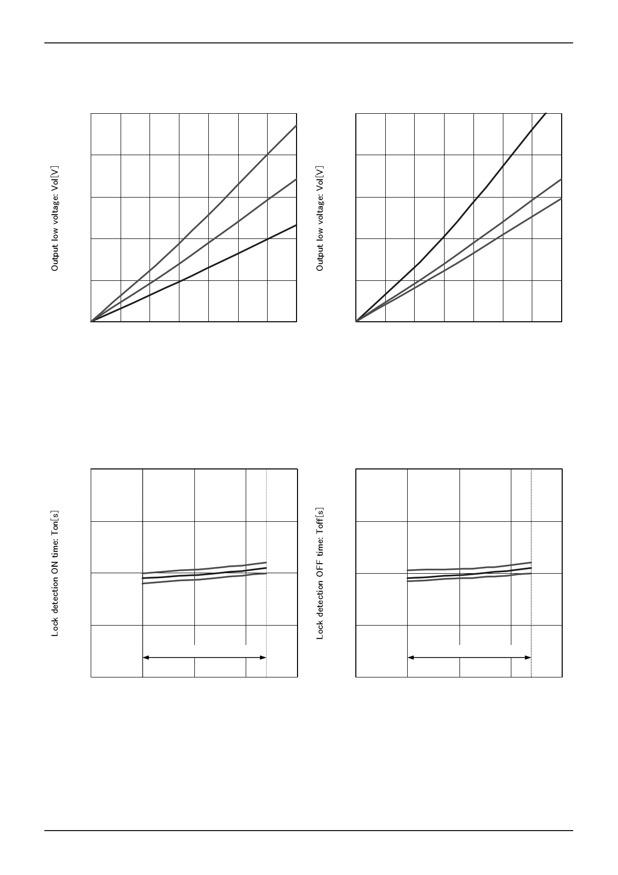
1.0 1.0
0.8
100°C
0.8
0.6
25°C
0.6
0.4 0.4
–40°C
0.2 0.2
5V
12V
17V
0.0
0.0
0.1 0.2 0.3 0.4 0.5 0.6
Output sink current: Io[A]
Fig.7 Output low voltage (Vcc=12V)
0.7
0.0
0.0
0.1 0.2 0.3 0.4 0.5 0.6
Output sink current: Io[A]
Fig.8 Output low voltage (Ta=25°C)
0.7
0.7 7.0
0.6 6.0
100°C
100°C
–40°C
–40°C
0.5
25°C
5.0
25°C
0.4
0.3
0
Operating range
5 10 15
Supply voltage: Vcc[V]
Fig.9 Lock detection ON time
4.0
Operating range
3.0
20 0
5 10 15
Supply voltage: Vcc[V]
20
Fig.10 Lock detection OFF time
www.rohm.com
© 2012 ROHM Co., Ltd. All rights reserved.
TSZ22111・15・001
5/13
TSZ02201-0H1H0B100170-1-2
28.JUL.2012 Rev.002
5 Page 
BD6721FS
Datasheet
●Power dissipation
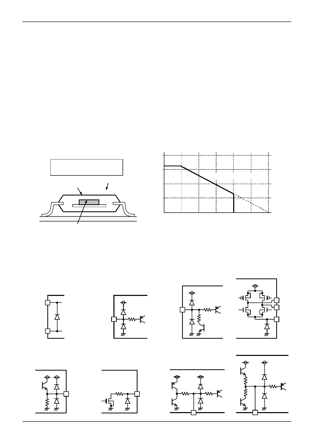
Power dissipation (total loss) indicates the power that can be consumed by IC at Ta=25°C (normal temperature). IC is
heated when it consumes power, and the temperature of IC chip becomes higher than ambient temperature. The
temperature that can be accepted by IC chip depends on circuit configuration, manufacturing process, etc, and consumable
power is limited. Power dissipation is determined by the temperature allowed in IC chip (maximum junction temperature)
and thermal resistance of package (heat dissipation capability). The maximum junction temperature is in general equal to
the maximum value in the storage temperature range.
Heat generated by consumed power of IC is radiated from the mold resin or lead frame of package. The parameter which
indicates this heat dissipation capability (hardness of heat release) is called heat resistance, represented by the symbol
θja[°C/W]. This heat resistance can estimate the temperature of IC inside the package. Fig.27 shows the model of heat
resistance of the package. Heat resistance θja, ambient temperature Ta, junction temperature Tj, and power consumption P
can be calculated by the equation below:
θja = (Tj – Ta) / P [°C/W]
Thermal de-rating curve indicates power that can be consumed by IC with reference to ambient temperature. Power that
can be consumed by IC begins to attenuate at certain ambient temperature. This gradient is determined by thermal
resistance θja. Thermal resistance θja depends on chip size, power consumption, package ambient temperature, packaging
condition, wind velocity, etc., even when the same package is used. Thermal de-rating curve indicates a reference value
measured at a specified condition. Fig.28 shows a thermal de-rating curve (Value when mounting FR4 glass epoxy board
70[mm] x 70[mm] x 1.6[mm] (copper foil area below 3[%])). Thermal resistance θjc from IC chip joint part to the package
surface part of mounting the above-mentioned same substrate is shown in the following as a reference value.
θjc = 43 [°C/W] (reference value)
Pd[mW]
θja = (Tj – Ta) / P [°C/W]
θjc = (Tj – Tc) / P [°C/W]
Ambient temperature Ta[°C]
Package surface temperature Tc[°C]
812.5
750
500
θja=153.8 [°C/W]
250
Chip surface temperature Tj[°C]
Power consumption P[W]
Fig.27 Thermal resistance
Ta[°C ]
0 25 50 75 100 125 150
*Reduce by 6.5mW/°C over 25°C
(On 70.0mm x 70.0mm x 1.6mm glass epoxy board)
Fig.28 Thermal de-rating curve
●I/O equivalence circuit(Resistance values are typical)
1) Power supply terminal,
2) Hall input terminals,
3) Minimum output duty setting
and Ground terminal
Output duty controllable input
terminal
terminal,
Output current detection
terminal, and
Level amplifier input terminal
Vcc
4) Motor output terminals,
and Output current
detecting resistor
connecting terminal
Vcc
Vcc
GND
H+
H–
TH
CS
LAIN
Vcc
1kΩ
MIN
1kΩ
30Ω
OUT1
OUT2
RNF
5) Reference voltage output
terminal
Vcc Vcc
6) Speed pulse signal output
terminal
Lock alarm signal output
terminal
7) Oscillating capacitor
connecting terminal
Vcc Vcc
31kΩ
REF
FG
20Ω AL
1kΩ 1kΩ
8) Level amplifier output
terminal
Vcc Vcc
45Ω
45Ω 1kΩ
www.rohm.com
© 2012 ROHM Co., Ltd. All rights reserved.
TSZ22111・15・001
11/13
OSC
LAOUT
TSZ02201-0H1H0B100170-1-2
28.JUL.2012 Rev.002
11 Page | ||
| Páginas | Total 17 Páginas | |
| PDF Descargar | [ Datasheet BD6721FS.PDF ] | |
Hoja de datos destacado
| Número de pieza | Descripción | Fabricantes |
| BD6721FS | Multifunction Single-phase Full-wave Fan Motor Driver | ROHM Semiconductor |
| Número de pieza | Descripción | Fabricantes |
| SLA6805M | High Voltage 3 phase Motor Driver IC. |
Sanken |
| SDC1742 | 12- and 14-Bit Hybrid Synchro / Resolver-to-Digital Converters. |
Analog Devices |
|
DataSheet.es es una pagina web que funciona como un repositorio de manuales o hoja de datos de muchos de los productos más populares, |
| DataSheet.es | 2020 | Privacy Policy | Contacto | Buscar |
