|
|
|
PDF 93AA76C Data sheet ( Hoja de datos )
| Número de pieza | 93AA76C | |
| Descripción | (93AA76A/B/C) 8K Microwire Compatible Serial EEPROM | |
| Fabricantes | Microchip Technology | |
| Logotipo | ||
Hay una vista previa y un enlace de descarga de 93AA76C (archivo pdf) en la parte inferior de esta página. Total 26 Páginas | ||
|
No Preview Available !
93AA76A/B/C, 93LC76A/B/C,
93C76A/B/C
8K Microwire Compatible Serial EEPROM
www.DataSheet4U.com
Device Selection Table
Part Number
93AA76A
93AA76B
93LC76A
93LC76B
93C76A
93C76B
93AA76C
93LC76C
93C76C
VCC Range
1.8-5.5
1.8-5-5
2.5-5.5
2.5-5.5
4.5-5.5
4.5-5.5
1.8-5.5
2.5-5.5
4.5-5.5
ORG Pin
No
No
No
No
No
No
Yes
Yes
Yes
PE Pin
No
No
No
No
No
No
Yes
Yes
Yes
Features
• Low-power CMOS technology
• ORG pin to select word size for ‘76C’ version
• 1024 x 8-bit organization ‘A’ devices (no ORG)
• 512 x 16-bit organization ‘B’ devices (no ORG)
• Program Enable pin to write-protect the entire
array (except on SOT-23 packages)
• Self-timed ERASE/WRITE cycles (including
auto-erase)
• Automatic ERAL before WRAL
• Power-on/off data protection circuitry
• Industry standard 3-wire serial I/O
• Device Status signal (READY/BUSY)
• Sequential READ function
• 1,000,000 E/W cycles
• Data retention > 200 years
• Temperature ranges supported:
- Industrial (I)
-40°C to +85°C
- Automotive (E)
-40°C to +125°C
Pin Function Table
Name
CS
CLK
DI
DO
VSS
PE
ORG
VCC
Function
Chip Select
Serial Data Clock
Serial Data Input
Serial Data Output
Ground
Program Enable
Memory Configuration
Power Supply
Word Size
8-bit
16-bit
8-bit
16-bit
8-bit
16-bit
8 or 16-bit
8 or 16-bit
8 or 16-bit
Temp Ranges
I
I
I, E
I, E
I, E
I, E
I
I, E
I, E
Packages
OT
OT
OT
OT
OT
OT
P, SN, ST, MS
P, SN, ST, MS
P, SN, ST, MS
Description
The Microchip Technology Inc. 93XX76A/B/C devices
are 8K bit, low-voltage, serial Electrically Erasable
PROMs (EEPROM). Word-selectable devices such as
the 93XX76C are dependent upon external logic
levels driving the ORG pin to set word size. For
dedicated 8-bit communication, the 93XX76A devices
are available, while the 93XX76B devices provide
dedicated 16-bit communication, available on SOT-23
devices only. A Program Enable (PE) pin allows the
user to write-protect the entire memory array.
Advanced CMOS technology makes these devices
ideal for low-power, nonvolatile memory applications.
The 93XX Series is available in standard packages
including 8-lead PDIP and SOIC, and advanced
packaging including 8-lead MSOP, 6-lead SOT-23,
and 8-lead TSSOP. Pb-free (Pure Matte Sn) finish is
also available.
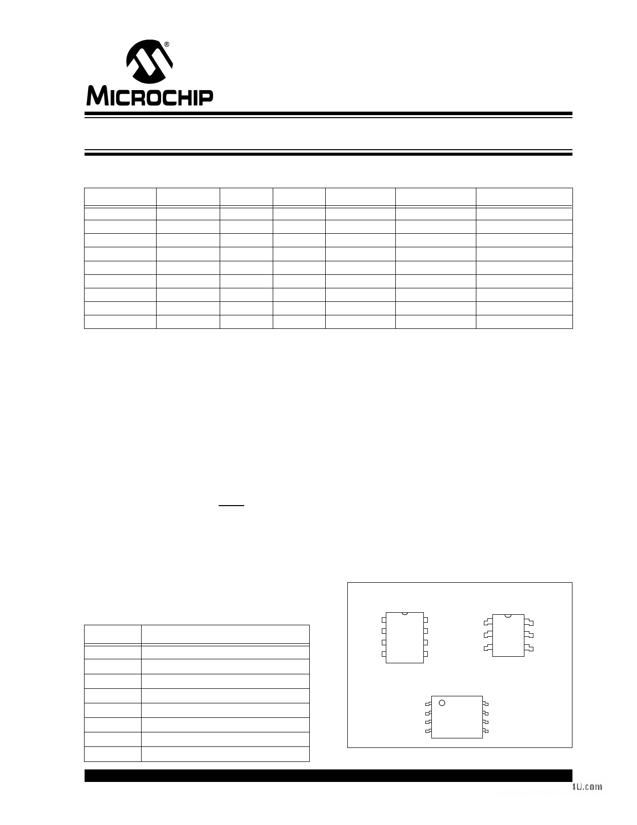
Package Types (not to scale)
PDIP/SOIC
(P, SN)
SOT-23
(OT)
CS
CLK
DI
DO
1
2
3
4
8 VCC
7 PE
6 ORG
5 VSS
DO 1
VSS 2
DI 3
6 VCC
5 CS
4 CLK
TSSOP/MSOP
(ST, MS)
CS
CLK
DI
DO
1
2
3
4
8 VCC
7 PE
6 ORG
5 VSS
2004 Microchip Technology Inc.
DS21796D-page 1
1 page 
93AA76A/B/C, 93LC76A/B/C, 93C76A/B/C
2.0 FUNCTIONAL DESCRIPTION
When the ORG* pin is connected to VCC, the (x16)
organization is selected. When it is connected to
ground, the (x8) organization is selected. Instructions,
addresses and write data are clocked into the DI pin on
the rising edge of the clock (CLK). The DO pin is
normally held in a HIGH-Z state except when reading
data from the device, or when checking the READY/
BUSY status during a programming operation. The
READY/BUSY status can be verified during an Erase/
Write operation by polling the DO pin; DO low indicates
that programming is still in progress, while DO high
indicates the device is ready. DO will enter the HIGH-Z
state on the falling edge of CS.
2.1 Start Condition
The Start bit is detected by the device if CS and DI are
both high with respect to the positive edge of CLK for
the first time.
Before a Start condition is detected, CS, CLK and DI
may change in any combination (except to that of a
Start condition), without resulting in any device
operation (READ, WRITE, ERASE, EWEN, EWDS,
ERAL or WRAL). As soon as CS is high, the device is
no longer in Standby mode.
An instruction following a Start condition will only be
executed if the required opcode, address and data bits
for any particular instruction are clocked in.
2.2 Data In/Data Out (DI/DO)
It is possible to connect the Data In and Data Out pins
together. However, with this configuration it is possible
for a “bus conflict” to occur during the “dummy zero”
that precedes the read operation, if A0 is a logic high-
level. Under such a condition the voltage level seen at
Data Out is undefined and will depend upon the relative
impedances of Data Out and the signal source driving
A0. The higher the current sourcing capability of the
driver, the higher the voltage at the Data Out pin. In
order to limit this current, a resistor should be
connected between DI and DO.
2.3 Data Protection
All modes of operation are inhibited when VCC is below
a typical voltage of 1.5V for ‘93AA’ and ‘93LC’ devices
or 3.8V for ‘93C’ devices.
The EWEN and EWDS commands give additional
protection against accidentally programming during
normal operation.
Note:
For added protection, an EWDS command
should be performed after every write
operation.
After power-up, the device is automatically in the
EWDS mode. Therefore, an EWEN instruction must be
performed before the initial ERASE or WRITE instruction
can be executed.
Block Diagram
VCC VSS
Memory
Array
Address
Decoder
DI
ORG*
CS
PE*
CLK
Data Register
Mode
Decode
Logic
Clock
Register
Address
Counter
Output DO
Buffer
*ORG and PE inputs are not available on
A/B devices.
2004 Microchip Technology Inc.
DS21796D-page 5
5 Page 
93AA76A/B/C, 93LC76A/B/C, 93C76A/B/C
3.0 PIN DESCRIPTIONS
TABLE 3-1:
Name
CS
CLK
DI
DO
VSS
ORG
PE
VCC
PIN DESCRIPTIONS
SOIC/PDIP/MSOP/
TSSOP
1
2
3
4
5
6
7
8
SOT-23
5
4
3
1
2
N/A
N/A
6
3.1 Chip Select (CS)
A high level selects the device; a low level deselects
the device and forces it into Standby mode. However, a
programming cycle which is already in progress will be
completed, regardless of the Chip Select (CS) input
signal. If CS is brought low during a program cycle, the
device will go into Standby mode as soon as the
programming cycle is completed.
CS must be low for 250 ns minimum (TCSL) between
consecutive instructions. If CS is low, the internal
control logic is held in a Reset status.
3.2 Serial Clock (CLK)
The Serial Clock is used to synchronize the communi-
cation between a master device and the 93XX series
device. Opcodes, address and data bits are clocked in
on the positive edge of CLK. Data bits are also clocked
out on the positive edge of CLK.
CLK can be stopped anywhere in the transmission
sequence (at high or low-level) and can be continued
anytime with respect to clock high time (TCKH) and
clock low time (TCKL). This gives the controlling master
freedom in preparing opcode, address and data.
CLK is a “don't care” if CS is low (device deselected). If
CS is high, but the Start condition has not been
detected (DI = 0), any number of clock cycles can be
received by the device without changing its status (i.e.,
waiting for a Start condition).
CLK cycles are not required during the self-timed
WRITE (i.e., auto ERASE/WRITE) cycle.
After detection of a Start condition the specified number
of clock cycles (respectively low to high transitions of
CLK) must be provided. These clock cycles are
required to clock in all required opcode, address and
data bits before an instruction is executed. CLK and DI
then become don't care inputs waiting for a new Start
condition to be detected.
Function
Chip Select
Serial Clock
Data In
Data Out
Ground
Organization / 93XX76C
Program Enable
Power Supply
3.3 Data In (DI)
Data In (DI) is used to clock in a Start bit, opcode,
address and data synchronously with the CLK input.
3.4 Data Out (DO)
Data Out (DO) is used in the Read mode to output data
synchronously with the CLK input (TPD after the
positive edge of CLK).
This pin also provides READY/BUSY status informa-
tion during ERASE and WRITE cycles. READY/BUSY
status information is available on the DO pin if CS is
brought high after being low for minimum Chip Select
low time (TCSL) and an erase or write operation has
been initiated.
The Status signal is not available on DO, if CS is held
low during the entire ERASE or WRITE cycle. In this
case, DO is in the HIGH-Z mode. If status is checked
after the ERASE/WRITE cycle, the data line will be high
to indicate the device is ready.
Note:
Issuing a Start bit and then taking CS low
will clear the READY/BUSY status from
DO.
3.5 Organization (ORG)
When the ORG pin is connected to VCC or Logic HI, the
(x16) memory organization is selected. When the ORG
pin is tied to VSS or Logic LO, the (x8) memory
organization is selected. For proper operation, ORG
must be tied to a valid logic level.
93XX76A devices are always x8 organization and
93XX76B devices are always x16 organization.
2004 Microchip Technology Inc.
DS21796D-page 11
11 Page | ||
| Páginas | Total 26 Páginas | |
| PDF Descargar | [ Datasheet 93AA76C.PDF ] | |
Hoja de datos destacado
| Número de pieza | Descripción | Fabricantes |
| 93AA76 | 8K/16K 1.8V Microwire Serial EEPROM | Microchip Technology |
| 93AA76-P | 8K/16K 1.8V Microwire Serial EEPROM | Microchip Technology |
| 93AA76-SN | 8K/16K 1.8V Microwire Serial EEPROM | Microchip Technology |
| 93AA76A | (93AA76A/B/C) 8K Microwire Compatible Serial EEPROM | Microchip Technology |
| Número de pieza | Descripción | Fabricantes |
| SLA6805M | High Voltage 3 phase Motor Driver IC. |
Sanken |
| SDC1742 | 12- and 14-Bit Hybrid Synchro / Resolver-to-Digital Converters. |
Analog Devices |
|
DataSheet.es es una pagina web que funciona como un repositorio de manuales o hoja de datos de muchos de los productos más populares, |
| DataSheet.es | 2020 | Privacy Policy | Contacto | Buscar |