|
|
PDF DS28CZ04 Data sheet ( Hoja de datos )
| Número de pieza | DS28CZ04 | |
| Descripción | EEPROM | |
| Fabricantes | Maxim Integrated Products | |
| Logotipo |  |
|
Hay una vista previa y un enlace de descarga de DS28CZ04 (archivo pdf) en la parte inferior de esta página. Total 22 Páginas | ||
|
No Preview Available !
www.maxim-ic.com
GENERAL DESCRIPTION
The DS28CZ04 combines 4kbit (512 x 8) EEPROM
with 4 PIO lines. Communication with the device is
accomplished with an industry standard I²C and
SMBus™ interface. The memory is organized as two
segments of 256 bytes with single byte and up to 16-
byte block write capability. Individual PIO lines may
be configured as inputs or outputs. The power-on
state of PIO programmed as outputs is stored in non-
volatile memory. All PIO may be reconfigured by the
user through the serial interface.
APPLICATIONS
• 4G SFP Copper Modules
• SFF-8472, SFP Fiber Modules
• RAID Systems
• Servers
TYPICALwww.DataSheet4U.com OPERATING CIRCUIT
VCCT
MOD-DEF2
MOD-DEF1
LOS
(from receiver)
VEET
VCC
DS28CZ04
SDA
SCL
MRZ
PIO3
PIO0
PIO2
WP PIO1
A2
A1 GND
From SFP
connector
VCC1
VCC2
MAX3982
PE1
PE0
OUTLEV
IN+
IN-
TX_DISABLE
LOS
OUT+
OUT-
LOSLEV
GND
VEET
EP
Connect to
VCC or GND
Small Form-factor Pluggable (SFP) Circuit
SMBus is a trademark of Intel Corp.
DS28CZ04
4kbit I²C/SMBus EEPROM
with Nonvolatile PIO
FEATURES
4kbit (512 x 8) EEPROM Organized in Two 256-
Byte Blocks
Single Byte and up to 16-Byte EEPROM Write
Sequences
Write-Protect Control Pin for the Entire EEPROM
Array
Endurance 200k Cycles per Block at 25°C; 10ms
max EEPROM Write Cycle
4 PIO Lines
Each PIO is Configured to Input or Output Mode
on Startup by Stored Value
All PIOs are Reconfigurable after Startup
Serial Interface User-Programmable for I²C Bus
and SMBus Compatibility
Supports 100kHz and 400kHz I²C Communica-
tion Speeds
Operating Range: 2.0V to 5.25V, -40°C to +85°C
4mm x 4mm 12-Pin TQFN Package
ORDERING INFORMATION
PART
DS28CZ04G-4+
DS28CZ04G-4+T
TEMP RANGE
-40°C to +85°C
-40°C to +85°C
PIN-PACKAGE
TQFN12-EP* 4x4mm²
TQFN12-EP* 4x4mm²
Tape-and-Reel
*EP = Exposed Paddle
+Denotes lead-free package.
PIN CONFIGURATION
12 11 10
A1 1
9 WP
A2 2
8 MRZ
PIO3 3
7 VCC
456
Thin 12-Lead 4mm × 4mm QFN (Top View)
Package Outline Drawing 21-0139
Package Code T1244+4
Note: Some revisions of this device may incorporate deviations from published specifications known as errata. Multiple revisions of any device
may be simultaneously available through various sales channels. For information about device errata, click here: www.maxim-ic.com/errata.
1 of 22
REV: 061107
1 page 
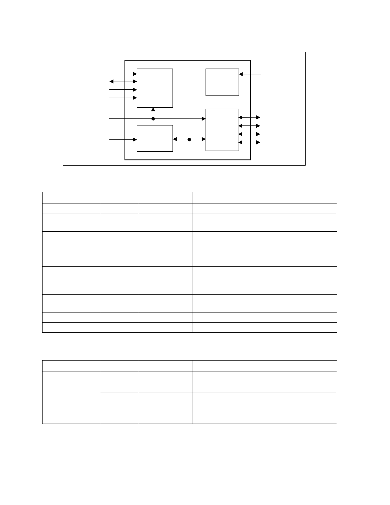
Figure 1. Block Diagram
SCL
SDA
A2
A1
MRZ
WP
DS28CZ04: 4kbit I²C/SMBus EEPROM with Nonvolatile PIO
Serial
Interface
Control
4-Kbit
EEPROM
Power
Distribu-
tion
PIO
Control
VCC
GND
PIO3
PIO2
PIO1
PIO0
Figure 2A. Memory Map (Device Address = A0h)
ADDRESS
00h to 74h
75h
76h
77h
78h to 79h
7Ah
7Bh
7Ch to 7Fh
80h to FFh
TYPE
EEPROM
EEPROM
EEPROM
EEPROM
⎯
SRAM
SRAM
SRAM
EEPROM
ACCESS
R/W
R/W
R/W
R/W
R
R/W
R/W
R/W
R/W
DESCRIPTION
User memory
Special function/user memory; controls whether
device powers-up into SFF Mode
Power-on default for PIO output state and
direction for all PIOs
Power-on default for PIO output type and read-
inversion for all PIOs
Reserved (reads FFh)
Direction setting for all PIOs and device
control/status register
PIO read-inversion and PIO output type for all
PIOs
PIO Read/Write Access Registers
User memory
Figure 2B. Memory Map (Device Address = A2h)
ADDRESS
00h to 6Dh
6Eh
6Fh to EFh
F0h to FFh
TYPE
EEPROM
EEPROM
⎯
EEPROM
⎯
ACCESS
R/W
R/W
R
R/W
R
DESCRIPTION
User memory
SFF Mode off: User memory
SFF Mode on: SFF Optional Status Register
User memory
Reserved (reads FFh)
5 of 22
5 Page 
DS28CZ04: 4kbit I²C/SMBus EEPROM with Nonvolatile PIO
As a 512 byte memory device, the DS28CZ04 needs 9 address bits to access a memory location. The P0 bit
transmitted in place of the A0 address bit specifies whether the “lower half” (0b) or the “upper half” (1b) of the
memory is addressed. This causes the DS28CZ04 to occupy two logical slave addresses, one for each half of the
memory. Throughout this document, the lower half of the memory is referenced as Device Address A0h and the
upper half as Device Address A2h. The addresses A0h and A2h are correct if the A1 and A2 pins are tied to logic
0. For different conditions at these pins the slave address changes accordingly.
The last bit of the slave-address/direction byte (R/W) defines the data direction. When set to a 0, subsequent data
will flow from master to slave (write access mode); when set to a 1, data will flow from slave to master (read access
mode). Although the P0 bit is also transmitted when accessing the DS28CZ04 in read mode, its value is ignored
(don’t care); instead, the value transmitted in the most recent write access applies.
I²C/SMBus Protocol
Data transfers may be initiated only when the bus is not busy. The master generates the serial clock (SCL),
controls the bus access, generates the START and STOP conditions, and determines the number of bytes
transferred on the data line (SDA) between START and STOP. Data is transferred in bytes with the most significant
bit being transmitted first. After each byte follows an acknowledge bit to allow synchronization between master and
slave. During any data transfer, SDA must remain stable whenever the clock line is HIGH. Changes in SDA line
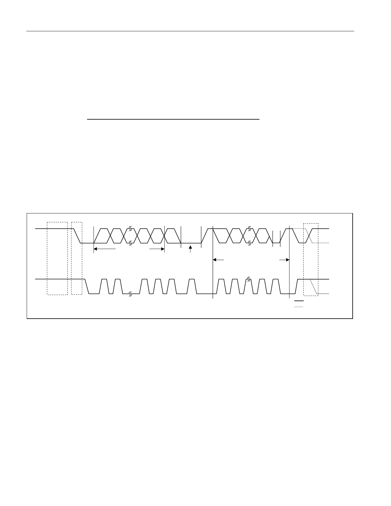
while SCL is high will be interpreted as a START or a STOP. The protocol is illustrated in Figure 5. For detailed
timing references see Figure 6.
Figure 5. I²C/SMBus Protocol Overview
MS-bit
R/W ACK
bit
SDA
Slave Address
Acknowledgment
from Receiver
ACK
bit
Repeated if more bytes
are transferred
SCL
Idle START
Condition
12
6 78
9
ACK
12
89
ACK
STOP Condition
Repeated START
Condition
Bus Idle or Not Busy
Both, SDA and SCL, are inactive, i. e., in their logic HIGH states.
START Condition
To initiate communication with a slave, the master has to generate a START condition. A START condition is
defined as a change in state of SDA from HIGH to LOW while SCL remains HIGH.
STOP Condition
To end communication with a slave, the master has to generate a STOP condition. A STOP condition is defined as
a change in state of SDA from LOW to HIGH while SCL remains HIGH.
Repeated START Condition
Repeated starts are commonly used for read accesses after having specified a memory address to read from in a
preceding write access. The master can use a repeated START condition at the end of a data transfer to
immediately initiate a new data transfer following the current one. A repeated START condition is generated the
same way as a normal START condition, but without leaving the bus idle after a STOP condition.
11 of 22
11 Page | ||
| Páginas | Total 22 Páginas | |
| PDF Descargar | [ Datasheet DS28CZ04.PDF ] | |
Hoja de datos destacado
| Número de pieza | Descripción | Fabricantes |
| DS28CZ04 | EEPROM | Maxim Integrated Products |
| Número de pieza | Descripción | Fabricantes |
| SLA6805M | High Voltage 3 phase Motor Driver IC. |
Sanken |
| SDC1742 | 12- and 14-Bit Hybrid Synchro / Resolver-to-Digital Converters. |
Analog Devices |
|
DataSheet.es es una pagina web que funciona como un repositorio de manuales o hoja de datos de muchos de los productos más populares, |
| DataSheet.es | 2020 | Privacy Policy | Contacto | Buscar |
