|
|
|
PDF DP83861 Data sheet ( Hoja de datos )
| Número de pieza | DP83861 | |
| Descripción | Gig PHYTER 10/100/1000 Ethernet Physical Layer | |
| Fabricantes | National Semiconductor | |
| Logotipo | ||
Hay una vista previa y un enlace de descarga de DP83861 (archivo pdf) en la parte inferior de esta página. Total 70 Páginas | ||
|
No Preview Available !
®
DP83861VQM-3 EN Gig PHYTER
10/100/1000 Ethernet Physical Layer
PRELIMINARY
April 2001
www.DataSheet4U.com
General Description
Features
The DP83861 is a full featured Physical Layer transceiver
with integrated PMD sublayers to support 10BASE-T,
100BASE-TX and 1000BASE-T Ethernet protocols.
The DP83861 uses state of the art 0.18 µm , 1.8 V/3.3 V
CMOS technology, fabricated at National Semiconductor’s
South Portland Maine facility.
The DP83861 is designed for easy implementation of
10/100/1000 Mb/s Ethernet LANs. It interfaces directly to
Twisted Pair media via an external transformer. This device
interfaces directly to the MAC layer through the IEEE
802.3u Standard Media Independent Interface (MII) or the
IEEE 802.3z Gigabit Media Independent Interface (GMII).
Applications
The DP83861 fits applications in:
s 10/100/1000 Mb/s capable node cards
s Switches with 10/100/1000 Mb/s capable ports
s High speed uplink ports (backbone)
s 100BASE-TX and 1000BASE-T compliant
s Fully compliant to IEEE 802.3u 100BASE-TX and IEEE
802.3z/ab 1000BASE-T specifications. Fully integrated
and fully compliant ANSI X3.T12 PMD physical sublayer
that includes adaptive equalization and Baseline Wan-
der compensation
s 10BASE-T compatible
s IEEE 802.3u Auto-Negotiation and Parallel Detection
– Fully Auto-Negotiates between 1000 Mb/s, 100 Mb/s,
and 10 Mb/s Full Duplex and Half Duplex devices
s Interoperates with first generation 1000BASE-T Physical
layer transceivers
s 3.3V MAC interfaces:
– IEEE 802.3u MII
– IEEE 802.3z GMII
s LED support: Link, Speed, Activity, Collision, TX and RX
s Supports 125 MHz or 25 MHz reference clock
s Requires only one 1.8 V and one 3.3 V supply
s Supports MDIX at 10, 100, and 1000 Mb/s
s Supports JTAG (IEEE1149.1)
s Dissipates 1 watt in 10/100 Mb/s mode
s Programmable Interrupts
s 208-pin PQFP package
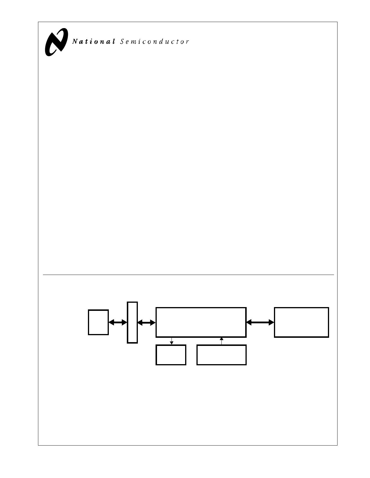
System Diagram
10BASE-T
100BASE-TX RJ-45
1000BASE-T
DP83861
10/100/1000Mb/s
Ethernet Physical Layer
MII/GMII
DP83820
10/100/1000Mb/s
ETHERNET
MAC
STATUS
LEDs
125 MHz or 25 MHz
CLOCK
PHYTER® is a registered trademark of National Semiconductor Corporation.
© 2001 National Semiconductor Corporation
www.national.com
1 page 
1.0 Pin Descriptions
The DP83861 pins are classified into the following interface
categories (each is described in the sections that follow):
— MAC Interface
— TP Interface
— JTAG Interface
— E2PROM Interface
— Clock Interface
— LED Interface
— Device Configuration / Strapping Options
— Reset
— Power and Ground Pins
— Special Connect Pins
Note: Strapping pin option (BOLD) (e.g. AN_EN)
1.1 MAC Interface
Type: I
Type: O
Type: O_Z
Type: I/O_Z
Type: S
Type: PU
Type: PD
Inputs
Output
Tristate Output
Tristate Input_Output
Strapping Pin
Pull-up
Pull-down
Signal Name
MDC
MDIO
CRS
COL
TX_CLK
TXD0
TXD1
TXD2
TXD3
TXD4
TXD5
TXD6
TXD7
TX_EN
GTX_CLK
Type
I
I/O
O
O
O
I
I
I
Pin #
151
150
111
110
130
146
145
144
141
140
139
138
135
134
147
Description
MANAGEMENT DATA CLOCK: Synchronous clock to the MDIO
management data input/output serial interface which may be asyn-
chronous to transmit and receive clocks. The maximum clock rate is
2.5 MHz with no minimum clock rate.
MANAGEMENT DATA I/O: Bi-directional management instruc-
tion/data signal that may be sourced by the station management en-
tity or the PHY. This pin requires a 1.5 kΩ pullup resistor.
CARRIER SENSE: Asserted high to indicate the presence of carrier
due to receive or transmit activity in Half Duplex mode. This signal is
not defined (LOW) for 1000BASE-T Full Duplex mode. For
1000BASE-T, 100BASE-TX and 10BASE-T Full Duplex operation
CRS is asserted only for receive activity.
COLLISION DETECT: Asserted high to indicate detection of a colli-
sion condition (assertion of CRS due to simultaneous transmit and re-
ceive activity) in Half Duplex modes. This signal is not synchronous
to either MII clock (GTX_CLK, TX_CLK or RX_CLK). This signal is not
defined (LOW) for Full Duplex modes.
TRANSMIT CLOCK (10 Mb/s and 100 Mb/s): Continuous clock sig-
nal generated from REF_CLK and driven by the PHY during 10Mb/s
and 100 Mb/s operation. It is used on the MII to clock all MII Transmit
(data, error) signals into the PHY.
The Transmit Clock frequency is constant and the frequency is
2.5 MHz for 10Mb/s mode and 25 MHz for 100Mb/s mode.
TX_CLK should not be confused with the TX_TCLK signal.
TRANSMIT DATA: These signals carry 4B data nibbles (TXD[3:0])
during 10 Mb/s and 100 Mb/s MII mode and 8-bit data (TXD[7:0]) in
1000 Mb/s GMII mode. They are synchronous to the Transmit Clocks
(TX_CLK, GTX_CLK. Transmit data is input enabled by TX_EN for all
modes all sourced by the controller.
TRANSMIT ENABLE: Active high input driven by the MAC request-
ing transmission of the data present on the TXD lines (nibble data for
10 Mb/s and 100 Mb/s mode and 8-bit data for 1000 Mb/s GMII
mode.)
GMII-TRANSMIT CLOCK: This continuous clock signal is sourced
from the upper level MAC to the PHY. Nominal frequency of 125 MHz,
derived in the MAC from its 125 MHz reference clock.
5 www.national.com
5 Page 
CD#_AGND
R#_AVDD#
R#_AGND#
R#_ASUB
11, 12, 41, 42
Common Driver Ground
2, 6, 17, 21, 32, 36, 47, 3.3V Receiver Analog Supply
51
3, 7, 16, 20, 33, 37, 46, Receiver Analog Ground
50
1, 22, 31, 52
Receiver Substrate Ground
INTERNAL SUPPLY PAIRS
Signal Name
PQFP Pin #
CORE_VDD
69, 83, 98, 129, 137,
160, 171, 182, 197
CORE_VSS
68, 82, 97, 128, 136,
161, 172, 183, 198
CORE_SUB
67, 96, 127, 162, 173,
199
PGM_AVDD
27
PGM_AGND
BG_SUB
BG_AVDD
BG_AGND
SHR_VDD
SHR_GND
OSC_VDD
OSC_VSS
28
26
23
25
29
30
155
152
1.8V Digital Supply
Description
Digital Ground
Substrate Ground
3.3V PGM/CGM Supply. We recommend a low pass RC filter of a
18-22 Ω resistor and a 22 µF capacitor connected to this pin.
PGM/CGM Ground
BG Substrate Ground
3.3V BG Supply
BG Ground
3.3V Share Logic Supply
Share Logic Ground
3.3V Oscillator Supply
Oscillator Ground
1.10 Special Connect Pins
Signal Name
PQFP Pin #
Description
BG_REF
24
Internal Reference Bias (requires connection to ground via a 9.31
kΩ resistor).
TEST
186, 206
These pins should be tied to 3.3 V.
SI,SO
104,105
These two pins should be floated.
RESERVE_FLOAT
(Please also see next row.
There are two sets of reserved
pins-- one set needs to be
pulled-down to gnd while the
other set needs to be floated.)
53-56, 59-62, 65, 66, 70,
71, 74-77, 80, 81, 84, 85,
88-91, 94, 95, 99, 100,
103,106, 107
These pins are reserved. These pins are to be left floating.
RESERVE_GND
165, 166, 169,
These pins are reserved and need to be tied to gnd.
170,174,175, 176,177
Note:I = Input, O = Output, I/O = Bidirectional, Z = Tri-state output, S = Strapping pin
11 www.national.com
11 Page | ||
| Páginas | Total 70 Páginas | |
| PDF Descargar | [ Datasheet DP83861.PDF ] | |
Hoja de datos destacado
| Número de pieza | Descripción | Fabricantes |
| DP83861 | DP83861 EN Gig PHYTER 10/100/1000 Ethernet Physical Layer (Rev. D) | Texas Instruments |
| DP83861 | Gig PHYTER 10/100/1000 Ethernet Physical Layer | National Semiconductor |
| DP83864 | DP83864 Quad GigPHYTER 10/100/1000 Ethernet Physical Layer (Rev. B) | Texas Instruments |
| DP83864 | Quad GigPHYTER 10/100/1000 Ethernet Physical Layer | National Semiconductor |
| Número de pieza | Descripción | Fabricantes |
| SLA6805M | High Voltage 3 phase Motor Driver IC. |
Sanken |
| SDC1742 | 12- and 14-Bit Hybrid Synchro / Resolver-to-Digital Converters. |
Analog Devices |
|
DataSheet.es es una pagina web que funciona como un repositorio de manuales o hoja de datos de muchos de los productos más populares, |
| DataSheet.es | 2020 | Privacy Policy | Contacto | Buscar |