|
|
|
PDF X1226 Data sheet ( Hoja de datos )
| Número de pieza | X1226 | |
| Descripción | Real Time Clock/Calendar | |
| Fabricantes | Intersil Corporation | |
| Logotipo | ||
Hay una vista previa y un enlace de descarga de X1226 (archivo pdf) en la parte inferior de esta página. Total 25 Páginas | ||
|
No Preview Available !
®
Data Sheet
X1226
4K (512 x 8), 2-Wire™ RTC
May 8, 2006
FN8098.3
Real Time Clock/Calendar with EEPROM
FEATURES
• Real Time Clock/Calendar
—Tracks Time in Hours, Minutes, and Seconds
—Day of the Week, Day, Month, and Year
• 2 Polled Alarms (Non-volatile)
—Settable on the Second, Minute, Hour, Day of
the Week, Day, or Month
—Repeat Mode (periodic interrupts)
• Oscillator Compensation On Chip
—Internal Feedback Resistor and Compensation
Capacitors
—64 Position Digitally Controlled Trim Capacitor
—6 Digital Frequency Adjustment Settings to
±30ppm
• Battery Switch or Super Cap Input
• 512 x 8 Bits of EEPROM
—64-Byte Page Write Mode
—8 Modes of Block Lock™ Protection
—Single Byte Write Capability
• High Reliability
—Data Retention: 100 Years
www.DataSheet4U.com — Endurance: 100,000 Cycles Per Byte
• 2-Wire™ Interface Interoperable with I2C
—400kHz Data Transfer Rate
• Frequency Output (SW Selectable: Off, 1Hz,
4096Hz or 32.768kHz)
• Low Power CMOS
—1.25µA Operating Current (Typical)
• Small Package Options
—8 Ld SOIC and 8 Ld TSSOP
• Repetitive Alarms
• Temperature Compensation
• Pb-Free Plus Anneal Available (RoHS Compliant)
APPLICATIONS
• Utility Meters
• HVAC Equipment
• Audio/Video Components
• Set Top Box/Television
• Modems
• Network Routers, Hubs, Switches, Bridges
• Cellular Infrastructure Equipment
• Fixed Broadband Wireless Equipment
• Pagers/PDA
• POS Equipment
• Test Meters/Fixtures
• Office Automation (Copiers, Fax)
• Home Appliances
• Computer Products
• Other Industrial/Medical/Automotive
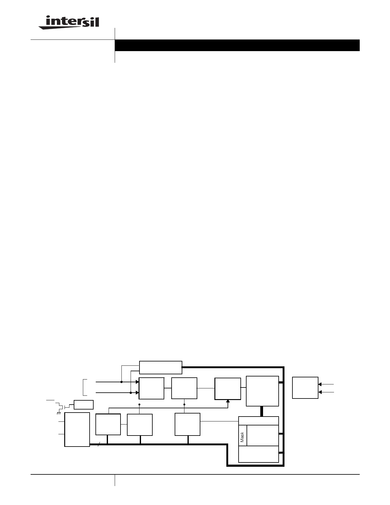
DESCRIPTION
The X1226 device is a Real Time Clock with
clock/calendar, two polled alarms with integrated
512x8 EEPROM, oscillator compensation, and battery
backup switch.
The oscillator uses an external, low-cost 32.768kHz
crystal. All compensation and trim components are
integrated on the chip. This eliminates several external
discrete components and a trim capacitor, saving
board area and component cost.
BLOCK DIAGRAM
OSC
Compensation
32.768kHz
X1
X2
PHZ/IRQ
Select
Oscillator
Frequency 1Hz
Divider
Timer
Calendar
Logic
Time
Keeping
Registers
(SRAM)
Battery
Switch
Circuitry
VCC
VBACK
SCL
SDA
Serial
Interface
Decoder
Control
Decode
Logic
8
Control/
Registers
(EEPROM)
Status
Registers
(SRAM)
Alarm
Compare
Alarm Regs
(EEPROM)
4K
EEPROM
ARRAY
1 CAUTION: These devices are sensitive to electrostatic discharge; follow proper IC Handling Procedures.
1-888-INTERSIL or 1-888-468-3774 | Intersil (and design) is a registered trademark of Intersil Americas Inc.
Copyright Intersil Americas Inc. 2005-2006. All Rights Reserved
All other trademarks mentioned are the property of their respective owners.
1 page 
X1226
POWER CONTROL OPERATION
The power control circuit accepts a VCC and a VBACK
input. The power control circuit powers the clock from
VBACK when VCC < VBACK – 0.2V. It will switch back to
power the device from VCC when VCC exceeds VBACK.
Figure 2. Power Control
VBACK
VCC
Off
Voltage
On
In
REAL TIME CLOCK OPERATION
The Real Time Clock (RTC) uses an external
32.768kHz quartz crystal to maintain an accurate inter-
nal representation of the second, minute, hour, day,
date, month, and year. The RTC has leap-year correc-
tion. The clock also corrects for months having fewer
than 31 days and has a bit that controls 24 hour or
AM/PM format. When the X1226 powers up after the
loss of both VCC and VBACK, the clock will not operate
until at least one byte is written to the clock register.
Reading the Real Time Clock
The RTC is read by initiating a Read command and
specifying the address corresponding to the register of
the Real Time Clock. The RTC Registers can then be
read in a Sequential Read Mode. Since the clock runs
continuously and a read takes a finite amount of time,
there is the possibility that the clock could change during
the course of a read operation. In this device, the time is
latched by the read command (falling edge of the clock
on the ACK bit prior to RTC data output) into a separate
latch to avoid time changes during the read operation.
The clock continues to run. Alarms occurring during a
read are unaffected by the read operation.
Writing to the Real Time Clock
The time and date may be set by writing to the RTC
registers. To avoid changing the current time by an
uncompleted write operation, the current time value is
loaded into a separate buffer at the falling edge of the
clock on the ACK bit before the RTC data input bytes,
the clock continues to run. The new serial input data
replaces the values in the buffer. This new RTC value
is loaded back into the RTC Register by a stop bit at
the end of a valid write sequence. An invalid write
operation aborts the time update procedure and the
contents of the buffer are discarded. After a valid write
operation the RTC will reflect the newly loaded data
beginning with the next “one second” clock cycle after
the stop bit is written. The RTC continues to update
the time while an RTC register write is in progress and
the RTC continues to run during any nonvolatile write
sequences. A single byte may be written to the RTC
without affecting the other bytes.
Accuracy of the Real Time Clock
The accuracy of the Real Time Clock depends on the
frequency of the quartz crystal that is used as the time
base for the RTC. Since the resonant frequency of a
crystal is temperature dependent, the RTC perfor-
mance will also be dependent upon temperature. The
frequency deviation of the crystal is a fuction of the
turnover temperature of the crystal from the crystal’s
nominal frequency. For example, a >20ppm frequency
deviation translates into an accuracy of >1 minute per
month. These parameters are available from the crystal
manufacturer. Intersil’s RTC family provides on-chip
crystal compensation networks to adjust load-
capacitance to tune oscillator frequency from +116 ppm
to -37 ppm when using a 12.5 pF load crystal. For more
detail information see the Application section.
CLOCK/CONTROL REGISTERS (CCR)
The Control/Clock Registers are located in an area
separate from the EEPROM array and are only
accessible following a slave byte of “1101111x” and
reads or writes to addresses [0000h:003Fh]. The
clock/control memory map has memory addresses
from 0000h to 003Fh. The defined addresses are
described in the Table 1. Writing to and reading from
the undefined addresses are not recommended.
CCR Access
The contents of the CCR can be modified by perform-
ing a byte or a page write operation directly to any
address in the CCR. Prior to writing to the CCR
(except the status register), however, the WEL and
RWEL bits must be set using a two step process (See
section “Writing to the Clock/Control Registers.”)
The CCR is divided into 5 sections. These are:
1. Alarm 0 (8 bytes; non-volatile)
2. Alarm 1 (8 bytes; non-volatile)
3. Control (4 bytes; non-volatile)
4. Real Time Clock (8 bytes; volatile)
5. Status (1 byte; volatile)
Each register is read and written through buffers. The
non-volatile portion (or the counter portion of the RTC) is
updated only if RWEL is set and only after a valid write
operation and stop bit. A sequential read or page write
operation provides access to the contents of only one
section of the CCR per operation. Access to another sec-
tion requires a new operation. Continued reads or writes,
5 FN8098.3
May 8, 2006
5 Page 
Figure 4. Valid Start and Stop Conditions
X1226
SCL
SDA
Start
Figure 5. Acknowledge Response From Receiver
SCL from
Master
Data Output
from Transmitter
Data Output
from Receiver
Start
1
DEVICE ADDRESSING
Following a start condition, the master must output a
Slave Address Byte. The first four bits of the Slave
Address Byte specify access to either the EEPROM
array or to the CCR. Slave bits ‘1010’ access the
EEPROM array. Slave bits ‘1101’ access the CCR.
When shipped from the factory, EEPROM array is
UNDEFINED, and should be programmed by the cus-
tomer to a known state.
Bit 3 through Bit 1 of the slave byte specify the device
select bits. These are set to ‘111’.
The last bit of the Slave Address Byte defines the
operation to be performed. When this R/W bit is a one,
then a read operation is selected. A zero selects a
write operation. Refer to Figure 6.
After loading the entire Slave Address Byte from the
SDA bus, the X1226 compares the device identifier
and device select bits with ‘1010111’ or ‘1101111’.
Upon a correct compare, the device outputs an
acknowledge on the SDA line.
Stop
89
Acknowledge
Following the Slave Byte is a two byte word address.
The word address is either supplied by the master
device or obtained from an internal counter. On power-
up the internal address counter is set to address 0h,
so a current address read of the EEPROM array starts
at address 0. When required, as part of a random
read, the master must supply the 2 Word Address
Bytes as shown in Figure 6.
In a random read operation, the slave byte in the
“dummy write” portion must match the slave byte in
the “read” section. That is if the random read is from
the array the slave byte must be 1010111x in both
instances. Similarly, for a random read of the
Clock/Control Registers, the slave byte must be
1101111x in both places.
11 FN8098.3
May 8, 2006
11 Page | ||
| Páginas | Total 25 Páginas | |
| PDF Descargar | [ Datasheet X1226.PDF ] | |
Hoja de datos destacado
| Número de pieza | Descripción | Fabricantes |
| X1226 | Real Time Clock/Calendar with EEPROM | Xicor |
| X1226 | Real Time Clock/Calendar | Intersil Corporation |
| X1227 | Real Time Clock/Calendar/CPU Supervisor with EEPROM | Xicor |
| X1227 | RTC Real TimeClock/Calendar/ CPU Supervisor | Intersil Corporation |
| Número de pieza | Descripción | Fabricantes |
| SLA6805M | High Voltage 3 phase Motor Driver IC. |
Sanken |
| SDC1742 | 12- and 14-Bit Hybrid Synchro / Resolver-to-Digital Converters. |
Analog Devices |
|
DataSheet.es es una pagina web que funciona como un repositorio de manuales o hoja de datos de muchos de los productos más populares, |
| DataSheet.es | 2020 | Privacy Policy | Contacto | Buscar |