|
|
|
PDF EL8173 Data sheet ( Hoja de datos )
| Número de pieza | EL8173 | |
| Descripción | (EL8170 / EL8173) Rail-to-Rail Input-Output Instrumentation Amplifiers | |
| Fabricantes | Intersil Corporation | |
| Logotipo | ||
Hay una vista previa y un enlace de descarga de EL8173 (archivo pdf) en la parte inferior de esta página. Total 14 Páginas | ||
|
No Preview Available !
DATASHEET
Micropower, Single Supply, Rail-to-Rail Input-Output
Instrumentation Amplifiers
EL8170, EL8173
The EL8170 and EL8173 are micropower instrumentation
amplifiers optimized for single supply operation over the
+2.4V to +5.5V range. Inputs and outputs can operate
rail-to-rail. As with all instrumentation amplifiers, a pair of
inputs provide very high common-mode rejection and are
completely independent from a pair of feedback terminals.
The feedback terminals allow zero input to be translated to any
output offset, including ground. A feedback divider controls the
overall gain of the amplifier.
The EL8170 is compensated for a gain of 100 or more, and the
EL8173 is compensated for a gain of 10 or more. The EL8170
and EL8173 have bipolar input devices for best offset and
1/f noise performance.
The amplifiers can be operated from one lithium cell or two
Ni-Cd batteries. The EL8170 and EL8173 input range includes
ground to slightly above positive rail. The output stage swings
to ground and positive supply (no pull-up or pull-down resistors
are needed).
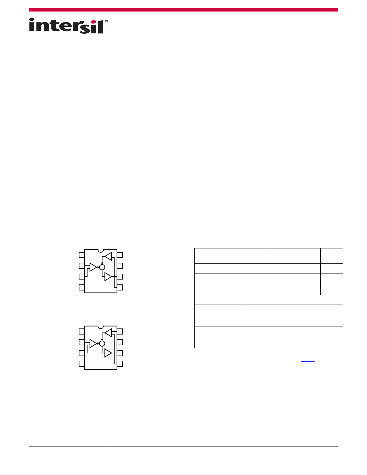
Pin Configurations
EL8170
(8 LD SOIC)
TOP VIEW
DNC 1
+- 8 FB+
IN- 2 +-
7 V+
IN+ 3
6 VOUT
V- 4
5 FB-
EL8173
(8 LD SOIC)
TOP VIEW
DNC 1
+- 8 FB+
IN- 2 +-
7 V+
IN+ 3
6 VOUT
V- 4
5 FB-
Features
• 95µA maximum supply current
• Maximum offset voltage
- 200µV (EL8170)
- 1000µV (EL8173)
• Maximum 3nA input bias current
• 396kHz -3dB bandwidth (G = 10)
• 192kHz -3dB bandwidth (G = 100)
• Single supply operation
- Input voltage range is rail-to-rail
- Output swings rail-to-rail
• Pb-Free (RoHS Compliant)
Applications
• Battery- or Solar-Powered Systems
• Strain Gauges
• Current Monitors
• Thermocouple Amplifiers
Ordering Information
PART NUMBER
(Notes 2, 3)
PART
MARKING
PACKAGE
(RoHS Compliant)
PKG.
DWG. #
EL8170FSZ (Note 1) 8170FSZ 8 Ld SOIC
M8.15E
EL8173FSZ (Note 1)
(No longer available
or supported)
8173FSZ 8 Ld SOIC
M8.15E
EL8170FWZ-EVAL
Evaluation Board
EL8173EV1Z (No
longer available or
supported)
Evaluation Board
EL8173FWZ-EVAL
Evaluation Board
(No longer available or
supported)
NOTES:
1. Add “-T*” suffix for tape and reel. Please refer to TB347 for details on
reel specifications.
2. These Intersil Pb-free plastic packaged products employ special
Pb-free material sets, molding compounds/die attach materials, and
100% matte tin plate plus anneal (e3 termination finish, which is
RoHS compliant and compatible with both SnPb and Pb-free
soldering operations). Intersil Pb-free products are MSL classified at
Pb-free peak reflow temperatures that meet or exceed the Pb-free
requirements of IPC/JEDEC J STD-020.
3. For Moisture Sensitivity Level (MSL), please see device information
page for EL8170, EL8173 For more information on MSL, please see
tech brief TB363.
August 11, 2015
FN7490.8
1
CAUTION: These devices are sensitive to electrostatic discharge; follow proper IC Handling Procedures.
1-888-INTERSIL or 1-888-468-3774 | Copyright Intersil Americas LLC 2009, 2013, 2015. All Rights Reserved
Intersil (and design) is a trademark owned by Intersil Corporation or one of its subsidiaries.
All other trademarks mentioned are the property of their respective owners.
1 page 
EL8170, EL8173
Typical Performance Curves V+ = +5V, V- = 0V, VCM = +2.5V, RL = Open, unless otherwise specified. (Continued)
120 90
80
100 70
80 CMRR
60
50 CMRR
60 40
30
40 20
20 10
0
0
10 100 1k 10k 100k 1M
FREQUENCY (Hz)
-1010
100 1k
10k 100k
FREQUENCY (Hz)
1M
FIGURE 7. EL8170 CMRR vs FREQUENCY
FIGURE 8. EL8173 CMRR vs FREQUENCY
140
120
PSRR+
100
80
PSRR-
60
40
20
0
10 100 1k 10k 100k
FREQUENCY (Hz)
FIGURE 9. EL8170 PSRR vs FREQUENCY
1M
90
80
PSRR+
70
60
PSRR-
50
40
30
20
10
0
10 100 1k 10k 100k
FREQUENCY (Hz)
FIGURE 10. EL8173 PSRR vs FREQUENCY
1M
250
200
150
100
501 10 100 1k 10k
FREQUENCY (Hz)
FIGURE 11. EL8170 VOLTAGE NOISE DENSITY
100k
2.5
2.0
1.5
1.0
0.5
0.0 1
10 100 1k 10k
FREQUENCY (Hz)
FIGURE 12. EL8173 VOLTAGE NOISE DENSITY
100k
Submit Document Feedback
5
FN7490.8
August 11, 2015
5 Page 
EL8170, EL8173
Input Bias Cancellation, Input
Bias Compensation
The EL8170 and EL8173 are features an Input Bias Cancellation
and Input Bias Compensation Circuit for both the input and
feedback terminals (IN+, IN-, FB+ and FB-), achieving a low input
bias current all throughout the input common-mode range and the
operating temperature range. While the PNP bipolar input stages
are biased with an adequate amount of biasing current for speed
and increased noise performance, the Input Bias Cancellation and
the Input Bias Compensation Circuit, sinks most of the base
current of the input transistor leaving a small portion as input bias
current, typically 500pA. In addition, the Input Bias Cancellation
and Input Bias Compensation Circuit, maintains a smooth and flat
behavior of the input bias current over the common mode range
and over the operating temperature range. The Input Bias
Cancellation and Input Bias Compensation Circuit, operates from
the input voltages of 10mV above the negative supply to the input
voltages slightly above the positive supply. See “Average Input Bias
Current vs Common-Mode Input Voltage” in the “Typical
Performance Curves” beginning on page 4.
Output Stage and Output Voltage Range
A pair of complementary MOSFET devices drives the output VOUT
to within a few millivolts of the supply rails. At a 100k load, the
PMOS sources current and pulls the output up to 4mV below the
positive supply, while the NMOS sinks current and pulls the
output down to 4mV above the negative supply, or ground in the
case of a single supply operation. The current sinking and
sourcing capability of the EL8170 and EL8173 are internally
limited to 26mA.
Gain Setting
VIN, the potential difference across IN+ and IN-, is replicated (less
the input offset voltage) across FB+ and FB-. The objective of the
EL8170 and EL8173 in-amp is to maintain the differential
voltage across FB+ and FB- equal to IN+ and IN-; (FB- - FB+) =
(IN+ - IN-). Consequently, the transfer function can be derived.
The gain of the EL8170 and EL8173 is set by two external
resistors, the feedback resistor RF, and the gain resistor RG.
VIN/2
VIN/2
VCM
+2.4V TO +5.5V
71
3 IN+ + V+
2 IN- - EL8170,
8 FB+ + EL8173
5 FB- - V-
4
6
VOUT
VOUT
=
1
+
R-R----G-F--
VI
N
(EQ. 1)
In Figure 37, the FB+ pin and one end of resistor RG are connected
to GND. With this configuration, Equation 1 is only true for a positive
swing in VIN; negative input swings will be ignored and the output
will be at ground.
Reference Connection
Unlike a three op amp instrumentation amplifier, a finite series
resistance seen at the REF terminal does not degrade the
EL8170 and EL8173's high CMRR performance, eliminating the
need for an additional external buffer amplifier. The circuit shown
in Figure 38 uses the FB+ pin as a REF terminal to center or to
adjust the output. Because the FB+ pin is a high impedance
input, an economical resistor divider can be used to set the
voltage at the REF terminal. The reference voltage error due to
the input bias current is minimized by keeping the values of the
voltage divider resistors, R1 and R2, as low as possible. Any
voltage applied to the REF terminal will shift VOUT by VREF times
the closed loop gain, which is set by resistors RF and RG
according to Equation 2. Note that any noise or unwanted signals
on the reference supply will be amplified at the output according
to Equation 2.
VOUT
=
1
+
R-R----G-F--
VIN
+
1
+
R-R----G-F--
VREF
(EQ. 2)
+2.4V TO +5.5V
VIN/2
VIN/2
+2.4V TO +5.5V
VCM
R1
REF
R2 RG
71
3 IN+ + V+
2 IN- - EL8170,
8 FB+ + EL8173
5 FB- - V-
4
6
RF
VOUT
FIGURE 38. GAIN SETTING AND REFERENCE CONNECTION
The FB+ pin can also be connected to the other end of resistor,
RG (see Figure 39). Keeping the basic concept that the EL8170
and EL8173 in-amps maintain constant differential voltage
across the input terminals and feedback terminals
(IN+ - IN- = FB+ - FB-), the transfer function of Figure 39 can be
derived (Equation 3). Note that the VREF gain term is eliminated,
and susceptibility to external noise is reduced.
RG RF
FIGURE 37. GAIN IS SET BY TWO EXTERNAL RESISTORS, RF
AND RG
Submit Document Feedback 11
FN7490.8
August 11, 2015
11 Page | ||
| Páginas | Total 14 Páginas | |
| PDF Descargar | [ Datasheet EL8173.PDF ] | |
Hoja de datos destacado
| Número de pieza | Descripción | Fabricantes |
| EL817 | 4 PIN DIP PHOTOTRANSISTOR PHOTOCOUPLER | Everlight Electronics |
| EL817-G | 4 PIN DIP PHOTOTRANSISTOR PHOTOCOUPLER | Everlight |
| EL8170 | (EL8170 / EL8173) Rail-to-Rail Input-Output Instrumentation Amplifiers | Intersil Corporation |
| EL8171 | (EL8171 / EL8172) Rail-to-Rail Input-Output Instrumentation Amplifiers | Intersil Corporation |
| Número de pieza | Descripción | Fabricantes |
| SLA6805M | High Voltage 3 phase Motor Driver IC. |
Sanken |
| SDC1742 | 12- and 14-Bit Hybrid Synchro / Resolver-to-Digital Converters. |
Analog Devices |
|
DataSheet.es es una pagina web que funciona como un repositorio de manuales o hoja de datos de muchos de los productos más populares, |
| DataSheet.es | 2020 | Privacy Policy | Contacto | Buscar |