|
|
|
PDF XU1005-BD Data sheet ( Hoja de datos )
| Número de pieza | XU1005-BD | |
| Descripción | GaAs MMIC Transmitter | |
| Fabricantes | Mimix Broadband | |
| Logotipo | ||
Hay una vista previa y un enlace de descarga de XU1005-BD (archivo pdf) en la parte inferior de esta página. Total 8 Páginas | ||
|
No Preview Available !
10.0-18.0 GHz GaAs MMIC
Transmitter
March 2007 - Rev 01-Mar-07
U1005-BD
Features
Integrated Mixer, LO Buffer and Output Amplifier
8 dB Conversion Gain
15 dB Image Rejection
+17 dBm OIP3
+6 dBm LO Drive Level
-12 dBm LO Leakage Power
100% On-Wafer RF and DC Testing
100% Visual Inspection to MIL-STD-883 Method 2010
General Description
Mimix Broadband's 10.0-18.0 GHz GaAs MMIC transmitter provides +17
dBm output third order intercept and 15 dB image rejection across the
band. This device is an image reject, balanced mixer followed by a two
stage output amplifier. The image reject mixer reduces the need for
unwanted sideband filtering before the power amplifier. I and Q mixer
inputs are provided and an external 90 degree hybrid is required to
select the desired sideband.This MMIC uses Mimix Broadband’s 0.15
µm GaAs PHEMT device model technology, and is based upon electron
beam lithography to ensure high repeatability and uniformity.The chip
has surface passivation to protect and provide a rugged part with
backside via holes and gold metallization to allow either a conductive
epoxy or eutectic solder die attach process.This device is well suited
for Millimeter-wave Point-to-Point Radio, LMDS, SATCOM and VSAT
applications.
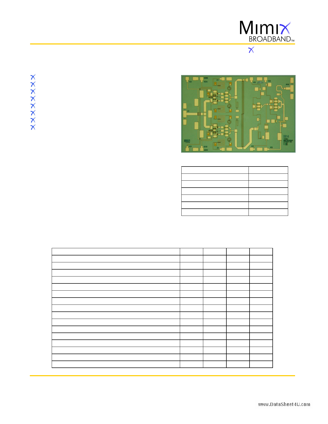
Chip Device Layout
XU1005-BD
Absolute Maximum Ratings
Supply Voltage (Vd)
Supply Current (Id1,2,3)
Gate Bias Voltage (Vg)
Input Power (IF Pin)
Storage Temperature (Tstg)
Operating Temperature (Ta)
Channel Temperature (Tch)
+6.0 VDC
250,150,250 mA
+0.3 VDC
0.0 dBm
-65 to +165 OC
-55 to MTTF Table1
MTTF Table1
(1) Channel temperature affects a device's MTTF. It is
recommended to keep channel temperature as low as
possible for maximum life.
Electrical Characteristics (Ambient Temperature T = 25o C)
Parameter
Units Min. Typ. Max.
Frequency Range (RF) Upper Side Band
GHz 10.0 - 18.0
Frequency Range (LO)
GHz 7.0
- 21.0
Frequency Range (IF)
GHz DC - 3.0
Output Return Loss RF (S22)
dB - 18.0 -
Small Signal Conversion Gain IF/RF (S21)
dB - 9.0 -
LO Input Drive (PLO)
dBm - +6.0 -
Isolation LO/RF
dB - 18.0 -
Output Third Order Intercept (OIP3)
dBm - +17.0 -
Drain Bias Voltage (Vd1,2,3)
VDC - +5.0 +5.5
Source Bias Voltage (Vs1)
VDC - -5.0 -
Gate Bias Voltage (Vg1), Mixer
VDC - -0.6 -
Gate Bias Voltage (Vg2,3)
VDC -1.2 -0.1 +0.1
Supply Current (Id1) (Vd1=5.0V)
mA - 140 200
Supply Current (Id2) (Vd2=5.0V, Vg=-0.1V Typical)
mA -
70 100
Supply Current (Id3) (Vd3=5.0V, Vg=-0.1V Typical)
mA - 140 200
Supply Current (Iss) (Vss=-5.0V)
mA - 140 200
Mimix Broadband, Inc., 10795 Rockley Rd., Houston, Texas 77099
Tel: 281.988.4600 Fax: 281.988.4615 mimixbroadband.com
Page 1 of 8
Characteristic Data and Specifications are subject to change without notice. ©2007 Mimix Broadband, Inc.
Export of this item may require appropriate export licensing from the U.S. Government. In purchasing these parts, U.S. Domestic customers accept
their obligation to be compliant with U.S. Export Laws.
1 page 
10.0-18.0 GHz GaAs MMIC
Transmitter
March 2007 - Rev 01-Mar-07
U1005-BD
App Note [1] Biasing - As shown in the bonding diagram, this device is operated by separately biasing Vd(1,2,3)=5.0V,
Vss=-5.0V, Id1=140mA, Id2=70mA, Id3=140mA and Is1=140mA. Additionally, a mixer is also required with Vg1=-0.6V.
Adjusting Vg1 above or below this value can adversely affect conversion gain, LO/RF isolation and intercept point
performance. Gain control can be adjusted by varying Vg2,3 from 0.0 to -1.2 V with 0.0V providing minimum
attenuation and -1.2 V providing maximum attenuation. It is also recommended to use active biasing to keep the
currents constant as the RF power and temperature vary; this gives the most reproducible results. Depending on the
supply voltage available and the power dissipation constraints, the bias circuit may be a single transistor or a low power
operational amplifier, with a low value resistor in series with the drain supply used to sense the current.The gate of the
pHEMT is controlled to maintain correct drain current and thus drain voltage.The typical gate voltage needed to do this
is -0.2V.Typically the gate is protected with Silicon diodes to limit the applied voltage. Also, make sure to sequence the
applied voltage to ensure negative gate bias is available before applying the positive drain supply.
App Note [2] Bias Arrangement -
For Parallel Stage Bias (Recommended for general applications) -- The same as Individual Stage Bias but all the drain or
gate pad DC bypass capacitors (~100-200 pF) can be combined. Additional DC bypass capacitance (~0.01 uF) is also
recommended to all DC or combination (if gate or drains are tied together) of DC bias pads.
For Individual Stage Bias -- Each DC pad (Vd1,2,3, Vss, and Vg1,2,3) needs to have DC bypass capacitance (~100-200 pF)
as close to the device as possible. Additional DC bypass capacitance (~0.01 uF) is also recommended.
MTTF Tables (TBD)
These numbers were calculated based on accelerated life test information and thermal model analysis received from the fabricating foundry.
Backplate
Temperature
Channel
Temperature
Rth
MTTF Hours
FITs
55 deg Celsius
deg Celsius
C/W
E+
E+
75 deg Celsius
deg Celsius
C/W
E+
E+
95 deg Celsius
deg Celsius
C/W
E+
E+
Bias Conditions: Vd1=Vd2=Vd3=5.0V, Vss=-5.0V, Id1=140mA, Id2=70mA, Id3=140mA, Is1=140mA
Mimix Broadband, Inc., 10795 Rockley Rd., Houston, Texas 77099
Tel: 281.988.4600 Fax: 281.988.4615 mimixbroadband.com
Page 5 of 8
Characteristic Data and Specifications are subject to change without notice. ©2007 Mimix Broadband, Inc.
Export of this item may require appropriate export licensing from the U.S. Government. In purchasing these parts, U.S. Domestic customers accept
their obligation to be compliant with U.S. Export Laws.
5 Page | ||
| Páginas | Total 8 Páginas | |
| PDF Descargar | [ Datasheet XU1005-BD.PDF ] | |
Hoja de datos destacado
| Número de pieza | Descripción | Fabricantes |
| XU1005-BD | GaAs MMIC Transmitter | Mimix Broadband |
| Número de pieza | Descripción | Fabricantes |
| SLA6805M | High Voltage 3 phase Motor Driver IC. |
Sanken |
| SDC1742 | 12- and 14-Bit Hybrid Synchro / Resolver-to-Digital Converters. |
Analog Devices |
|
DataSheet.es es una pagina web que funciona como un repositorio de manuales o hoja de datos de muchos de los productos más populares, |
| DataSheet.es | 2020 | Privacy Policy | Contacto | Buscar |