|
|
|
PDF XP1018-BD Data sheet ( Hoja de datos )
| Número de pieza | XP1018-BD | |
| Descripción | GaAs MMIC Power Amplifier | |
| Fabricantes | Mimix Broadband | |
| Logotipo | ||
Hay una vista previa y un enlace de descarga de XP1018-BD (archivo pdf) en la parte inferior de esta página. Total 8 Páginas | ||
|
No Preview Available !
37.0-42.0 GHz GaAs MMIC
Power Amplifier
February 2007 - Rev 01-Feb-07
Features
Excellent Transmit Output Stage
Output Power Adjust
26.0 dB Small Signal Gain
+25.0 dBm P1dB Compression Point
100% On-Wafer RF, DC and Output Power Testing
100% Visual Inspection to MIL-STD-883
Method 2010
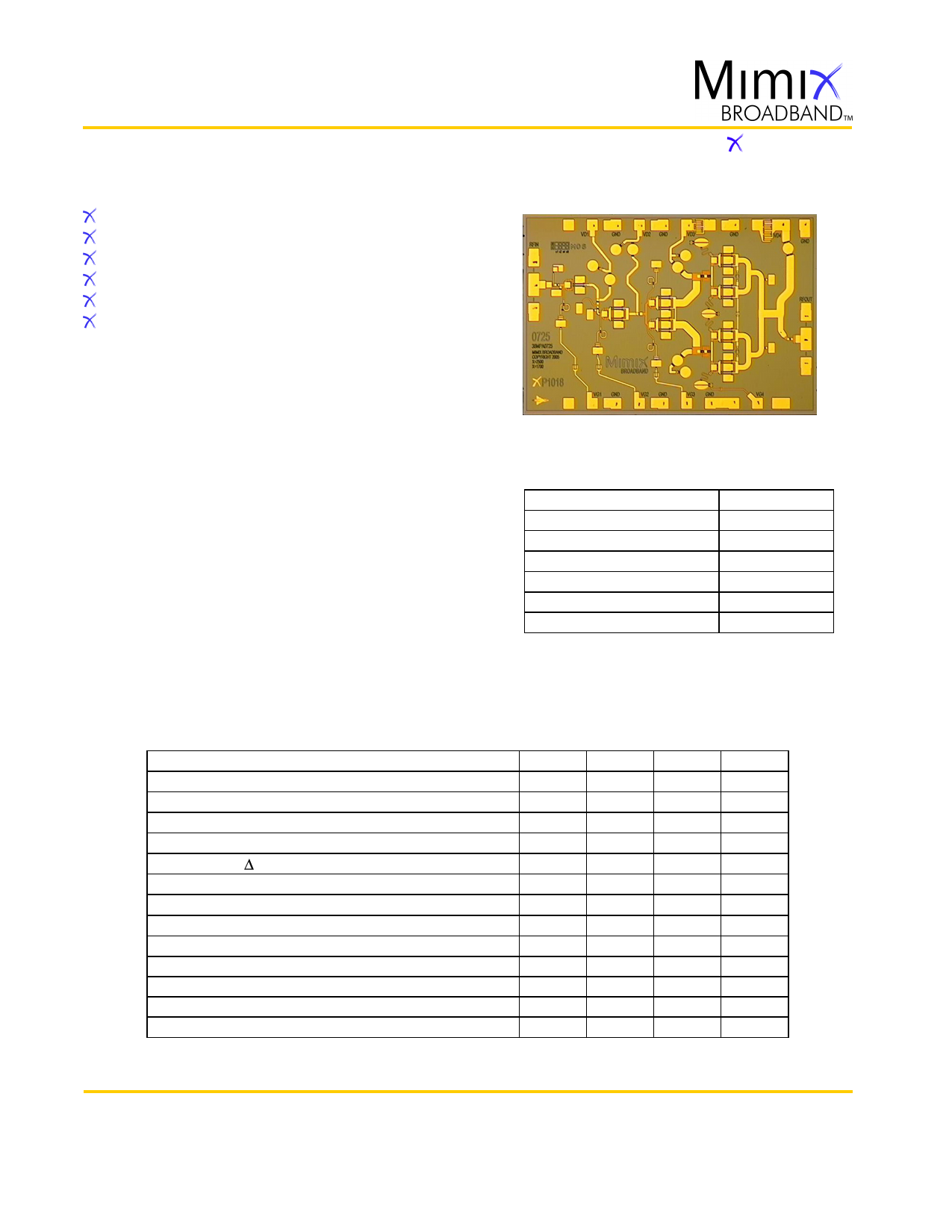
P1018-BD
Chip Device Layout
General Description
Mimix Broadband’s four stage 37.0-42.0 GHz GaAs
MMIC power amplifier has a small signal gain of 26.0
dB with a +25.0 dBm P1dB output compression point.
This MMIC uses Mimix Broadband’s 0.15 µm GaAs
PHEMT device model technology, and is based upon
electron beam lithography to ensure high
repeatability and uniformity.The chip has surface
passivation to protect and provide a rugged part with
backside via holes and gold metallization to allow
either a conductive epoxy or eutectic solder die
www.DataSheet4U.com
attach process.This device is well suited for
Millimeter-wave Point-to-Point Radio, LMDS, SATCOM
and VSAT applications.
Absolute Maximum Ratings
Supply Voltage (Vd)
Supply Current (Id1,2,3,4)
Gate Bias Voltage (Vg)
Input Power (Pin)
Storage Temperature (Tstg)
Operating Temperature (Ta)
Channel Temperature (Tch)
+6.0 VDC
45,80,165,325 mA
+0.3 VDC
TBD
-65 to +165 OC
-55 to MTTF Table1
MTTF Table1
(1) Channel temperature affects a device's MTTF. It is
recommended to keep channel temperature as low as
possible for maximum life.
Electrical Characteristics (Ambient Temperature T = 25 oC)
Parameter
Frequency Range (f )
Input Return Loss (S11)
Output Return Loss (S22)
Small Signal Gain (S21)
Gain Flatness ( S21)
Reverse Isolation (S12)
Output Power for 1dB Compression (P1dB) 2
Drain Bias Voltage (Vd1,2,3,4)
Gate Bias Voltage (Vg1,2,3,4)
Supply Current (Id1) (Vd=5.0V, Vg=-0.7V Typical)
Supply Current (Id2) (Vd=5.0V, Vg=-0.7V Typical)
Supply Current (Id3) (Vd=5.0V, Vg=-0.7V Typical)
Supply Current (Id4) (Vd=5.0V, Vg=-0.7V Typical)
(2) Measured using constant current.
Units Min. Typ. Max.
GHz 37.0 - 42.0
dB - 9.0 -
dB - 10.0 -
dB - 26.0 -
dB - +/-1.5 -
dB - 45.0 -
dBm - +25.0 -
VDC - +5.0 +5.5
VDC -1.0 -0.7 0.0
mA - 35 40
mA - 60 70
mA - 125 150
mA - 245 295
Mimix Broadband, Inc., 10795 Rockley Rd., Houston, Texas 77099
Tel: 281.988.4600 Fax: 281.988.4615 mimixbroadband.com
Page 1 of 8
Characteristic Data and Specifications are subject to change without notice. ©2007 Mimix Broadband, Inc.
Export of this item may require appropriate export licensing from the U.S. Government. In purchasing these parts, U.S. Domestic customers accept
their obligation to be compliant with U.S. Export Laws.
1 page 
37.0-42.0 GHz GaAs MMIC
Power Amplifier
February 2007 - Rev 01-Feb-07
P1018-BD
App Note [1] Biasing - It is recommended to separately bias each amplifier stage Vd1 through Vd4 at Vd(1,2,3,4)=5.0V with Id1=35mA, Id2=60mA,
Id3=125mA and Id4=245mA. Separate biasing is recommended if the amplifier is to be used at high levels of saturation, where gate rectification will
alter the effective gate control voltage. For non-critical applications it is possible to parallel all stages and adjust the common gate voltage for a
total drain current Id(total)=465 mA. It is also recommended to use active biasing to keep the currents constant as the RF power and temperature
vary; this gives the most reproducible results. Depending on the supply voltage available and the power dissipation constraints, the bias circuit may
be a single transistor or a low power operational amplifier, with a low value resistor in series with the drain supply used to sense the current.The
gate of the pHEMT is controlled to maintain correct drain current and thus drain voltage. The typical gate voltage needed to do this is -0.7V.
Typically the gate is protected with Silicon diodes to limit the applied voltage. Also, make sure to sequence the applied voltage to ensure negative
gate bias is available before applying the positive drain supply.
App Note [2] Bias Arrangement -
For Parallel Stage Bias (Recommended for general applications) -- The same as Individual Stage Bias but all the drain or gate pad DC bypass
capacitors (~100-200 pF) can be combined. Additional DC bypass capacitance (~0.01 uF) is also recommended to all DC or combination (if gate or
drains are tied together) of DC bias pads.
For Individual Stage Bias (Recommended for saturated applications) -- Each DC pad (Vd1,2,3,4 and Vg1,2,3,4) needs to have DC bypass capacitance
(~100-200 pF) as close to the device as possible. Additional DC bypass capacitance (~0.01 uF) is also recommended.
App Note [3] Output Power Adjust Using Gate Control - This device has a very useful additional feature.The output power can be adjusted by
lowering the individual or combined gate voltages towards pinch off without sacrificing much in the way of Input/Output 3rd Order Intercept Point.
Improvements to the IIP3/OIP3 data shown here while attenuating the gain are also possible with individual gate control. Data here has been taken
using combined gate control (all gates changed together) to lower the device's output power.The results are shown below. Additionally, the
accompanying graphs show the level and linearity of the typical attenuation achievable as the gate is adjusted at various levels until pinch-off.
XP1018-BD: Pout vs. Vd @ 40 GHz and Pin=+5dBm
20
10
0
-10
-20
-30
-40
-50
0 0.5 1 1.5 2 2.5 3 3.5 4 4.5
Drain voltage (V)
Mimix Broadband, Inc., 10795 Rockley Rd., Houston, Texas 77099
Tel: 281.988.4600 Fax: 281.988.4615 mimixbroadband.com
Page 5 of 8
Characteristic Data and Specifications are subject to change without notice. ©2007 Mimix Broadband, Inc.
Export of this item may require appropriate export licensing from the U.S. Government. In purchasing these parts, U.S. Domestic customers accept
their obligation to be compliant with U.S. Export Laws.
5 Page | ||
| Páginas | Total 8 Páginas | |
| PDF Descargar | [ Datasheet XP1018-BD.PDF ] | |
Hoja de datos destacado
| Número de pieza | Descripción | Fabricantes |
| XP1018-BD | GaAs MMIC Power Amplifier | Mimix Broadband |
| Número de pieza | Descripción | Fabricantes |
| SLA6805M | High Voltage 3 phase Motor Driver IC. |
Sanken |
| SDC1742 | 12- and 14-Bit Hybrid Synchro / Resolver-to-Digital Converters. |
Analog Devices |
|
DataSheet.es es una pagina web que funciona como un repositorio de manuales o hoja de datos de muchos de los productos más populares, |
| DataSheet.es | 2020 | Privacy Policy | Contacto | Buscar |