|
|
|
PDF EM636165-XXI Data sheet ( Hoja de datos )
| Número de pieza | EM636165-XXI | |
| Descripción | 1Mega x 16 Synchronous DRAM | |
| Fabricantes | Etron Technology | |
| Logotipo | ||
Hay una vista previa y un enlace de descarga de EM636165-XXI (archivo pdf) en la parte inferior de esta página. Total 30 Páginas | ||
|
No Preview Available !
EtronTech
EM636165-XXI
1Mega x 16 Synchronous DRAM (SDRAM)
Preliminary (Rev. 1.1, 04/2005)
Features
• Fast access time: 5/5.5/6.5/7.5 ns
• Fast clock rate: 166/143/125/100 MHz
• Self refresh mode: standard and low power
• Internal pipelined architecture
• 512K word x 16-bit x 2-bank
• Programmable Mode registers
- CAS# Latency: 1, 2, or 3
- Burst Length: 1, 2, 4, 8, or full page
- Burst Type: interleaved or linear burst
- Burst stop function
• Individual byte controlled by LDQM and UDQM
• Auto Refresh and Self Refresh
• 4096 refresh cycles/64ms
• CKE power down mode
• Single +3.3V±0.3V power supply
• Interface: LVTTL
• 50-pin 400 mil plastic TSOP II package
• Lead Free Package available
Key Specifications
tCK3
tRAS
tAC3
tRC
EM636165
Clock Cycle time(min.)
Row Active time(max.)
Access time from CLK(max.)
Row Cycle time(min.)
-6I/7I/8I/10I
6/7/8/10ns
36/42/48/60 ns
5/5.5/6.5/7.5 ns
54/63/72/90 ns
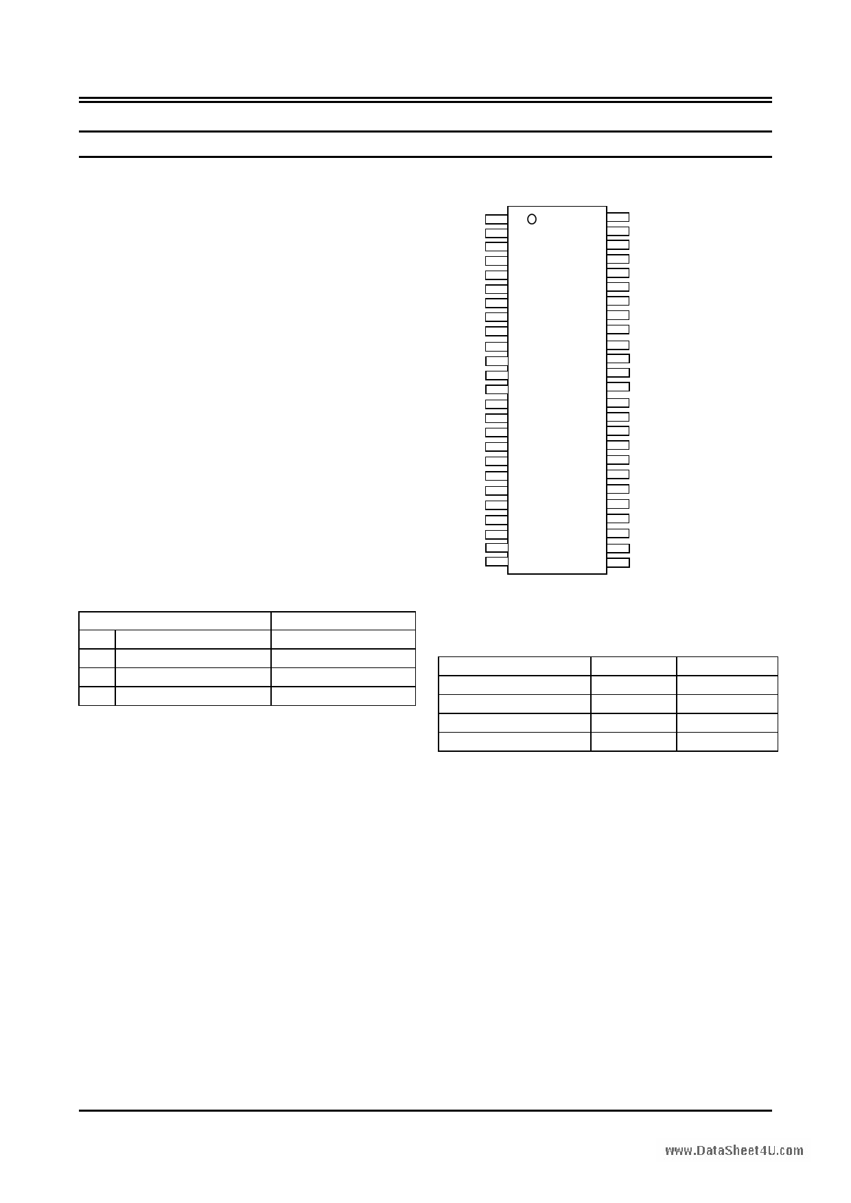
Pin Assignment (Top View)
VDD
DQ0
DQ1
VSSQ
DQ2
DQ3
VDDQ
DQ4
DQ5
VSSQ
DQ6
DQ7
VDDQ
LDQM
WE#
CAS#
RAS#
CS#
A11
A10
A0
A1
A2
A3
VDD
1
2
3
4
5
6
7
8
9
10
11
12
13
14
15
16
17
18
19
20
21
22
23
24
25
50 Vss
49 DQ15
48 DQ14
47 VSSQ
46 DQ13
45 DQ12
44 VDDQ
43 DQ11
42 DQ10
41 VSSQ
40 DQ9
39 DQ8
38 VDDQ
37 NC
36 UDQM
35 CLK
34 CKE
33 NC
32 A9
31 A8
30 A7
29 A6
28 A5
27 A4
26 Vss
Ordering Information
Industrial Operating temperature: -40~85°C
Part Number
Frequency
EM636165TS-6I/6IG
166MHz
EM636165TS-7I/7IG
143MHz
EM636165TS-8I/8IG
125MHz
EM636165TS-10I/10IG
100MHz
G : indicates Lead Free Package
Package
TSOP II
TSOP II
TSOP II
TSOP II
Overview
The EM636165 SDRAM is a high-speed CMOS synchronous DRAM containing 16 Mbits. It is internally configured
as a dual 512K word x 16 DRAM with a synchronous interface (all signals are registered on the positive edge of the
clock signal, CLK). Each of the 512K x 16 bit banks is organized as 2048 rows by 256 columns by 16 bits. Read and
write accesses to the SDRAM are burst oriented; accesses start at a selected location and continue for a programmed
number of locations in a programmed sequence. Accesses begin with the registration of a BankActivate command
which is then followed by a Read or Write command.
The EM636165 provides for programmable Read or Write burst lengths of 1, 2, 4, 8, or full page, with a burst
termination option. An auto precharge function may be enabled to provide a self-timed row precharge that is initiated at
the end of the burst sequence. The refresh functions, either Auto or Self Refresh are easy to use. By having a
programmable mode register, the system can choose the most suitable modes to maximize its performance. These
Etron Technology, Inc.
No. 6, Technology Road V, Science-Based Industrial Park, Hsinchu, Taiwan 30077, R.O.C
TEL: (886)-3-5782345
FAX: (886)-3-5778671
Etron Technology, Inc., reserves the right to make changes to its products and specifications without notice.
1 page 
EtronTech
1M x 16 SDRAM EM636165-XXI
Operation Mode
Fully synchronous operations are performed to latch the commands at the positive edges of CLK.
Table 2 shows the truth table for the operation commands.
Table 2. Truth Table (Note (1), (2) )
Command
State CKEn-1 CKEn DQM(6) A11 A10 A0-9 CS# RAS# CAS# WE#
BankActivate
Idle(3) H X
X VV V L L H H
BankPrecharge
Any H X X V L X L L H L
PrechargeAll
Any H X X X H X L L H L
W rite
Active(3) H
X
X VL V L H L L
Write and AutoPrecharge
Active(3) H
X
X VH V L H L L
Read
Active(3) H
X
X VL V L H L H
Read and Autoprecharge
Active(3) H
X
X VH V L H L H
Mode Register Set
Idle H X X V V V L L L L
No-Operation
Any H X X X X X L H H H
Burst Stop
Active(4) H
X
X XX X L H H L
Device Deselect
Any H X X X X X H X X X
AutoRefresh
Idle H H X X X X L L L H
SelfRefresh Entry
Idle H L X X X X L L L H
SelfRefresh Exit
Idle
LH
X XX X H X X X
(SelfRefresh)
LH HH
Clock Suspend Mode Entry
Active H L
X XX X X X X X
Power Down Mode Entry
Any(5) H L
X XX X H X X X
LH HH
Clock Suspend Mode Exit
Active L H
X XX X X X X X
Power Down Mode Exit
Any
LH
X XX X H X X X
(PowerDown)
LH HH
Data Write/Output Enable
Active H X
L XX X X X X X
Data Mask/Output Disable
Active H X H X X X X X X
Note:
1. V=Valid X=Don't Care L=Low level H=High level
2. CKEn signal is input level when commands are provided.
CKEn-1 signal is input level one clock cycle before the commands are provided.
3. These are states of bank designated by BS signal.
4. Device state is 1, 2, 4, 8, and full page burst operation.
5. Power Down Mode can not enter in the burst operation.
When this command is asserted in the burst cycle, device state is clock suspend mode.
6. LDQM and UDQM
X
Preliminary
5 Rev. 1.1 Apr. 2005
5 Page 
EtronTech
1M x 16 SDRAM EM636165-XXI
6 Write and AutoPrecharge command (refer to the following figure)
(RAS# = "H", CAS# = "L", WE# = "L", A11 = “V”, A10 = "H", A0-A7 = Column Address)
The Write and AutoPrecharge command performs the precharge operation automatically after
the write operation. Once this command is given, any subsequent command can not occur within a
time delay of {(burst length -1) + tWR + tRP(min.)}. At full-page burst, only the write operation is
performed in this command and the auto precharge function is ignored.
T0 T1
T2 T3
T4 T5
T6 T7
T8
CLK
C OM M A ND
Bank A
Activate
CAS# latency=1
tCK1, DQ's
CAS# latency=2
tCK2, DQ's
CAS# latency=3
tCK3, DQ's
NOP
NOP
Write A
AutoPrecharge
DIN A0
DIN A0
NOP
DIN A1
DIN A1
NOP
tDAL
*
tDAL
*
DIN A0
DIN A1
*
NOP
tDAL
NOP
NOP
tDAL= tWR + tRP
* Begin AutoPrecharge
Bank can be reactivated at completion of tDAL
Burst Write with Auto-Precharge (Burst Length = 2, CAS# Latency = 1, 2, 3)
7 Mode Register Set command
(RAS# = "L", CAS# = "L", WE# = "L", A11 = “V”, A10 = “V”, A0-A9 = Register Data)
The mode register stores the data for controlling the various operating modes of SDRAM. The
Mode Register Set command programs the values of CAS# latency, Addressing Mode and Burst
Length in the Mode register to make SDRAM useful for a variety of different applications. The
default values of the Mode Register after power-up are undefined; therefore this command must be
issued at the power-up sequence. The state of pins A0~A9 and A11 in the same cycle is the data
written to the mode register. One clock cycle is required to complete the write in the mode register
(refer to the following figure). The contents of the mode register can be changed using the same
command and the clock cycle requirements during operation as long as both banks are in the idle
state.
Preliminary
11 Rev. 1.1 Apr. 2005
11 Page | ||
| Páginas | Total 30 Páginas | |
| PDF Descargar | [ Datasheet EM636165-XXI.PDF ] | |
Hoja de datos destacado
| Número de pieza | Descripción | Fabricantes |
| EM636165-XXI | 1Mega x 16 Synchronous DRAM | Etron Technology |
| Número de pieza | Descripción | Fabricantes |
| SLA6805M | High Voltage 3 phase Motor Driver IC. |
Sanken |
| SDC1742 | 12- and 14-Bit Hybrid Synchro / Resolver-to-Digital Converters. |
Analog Devices |
|
DataSheet.es es una pagina web que funciona como un repositorio de manuales o hoja de datos de muchos de los productos más populares, |
| DataSheet.es | 2020 | Privacy Policy | Contacto | Buscar |