|
|
|
PDF FDMB506P Data sheet ( Hoja de datos )
| Número de pieza | FDMB506P | |
| Descripción | P-Channel 1.8V Logic Level PowerTrench MOSFET | |
| Fabricantes | Fairchild Semiconductor | |
| Logotipo | ||
Hay una vista previa y un enlace de descarga de FDMB506P (archivo pdf) en la parte inferior de esta página. Total 6 Páginas | ||
|
No Preview Available !
December 2005
FDMB506P
P-Channel 1.8V Logic Level PowerTrench MOSFET
General Description
This P-Channel MOSFET is produced using Fairchild
Semiconductor’s advanced PowerTrench process that
has been especially tailored to minimize the on-state
resistance and yet maintain low gate charge for
superior switching performance. These devices are
well suited for portable electronics applications.
Applications
• Load switch
• DC/DC Conversion
Features
• –6.8 A, –20V. RDS(ON) = 30 mΩ @ VGS = –4.5V
RDS(ON) = 38 mΩ @ VGS = –2.5V
RDS(ON) = 70 mΩ @ VGS = –1.8V
• Low profile – 0.8 mm maximum
• Fast switching
• RoHS compliant
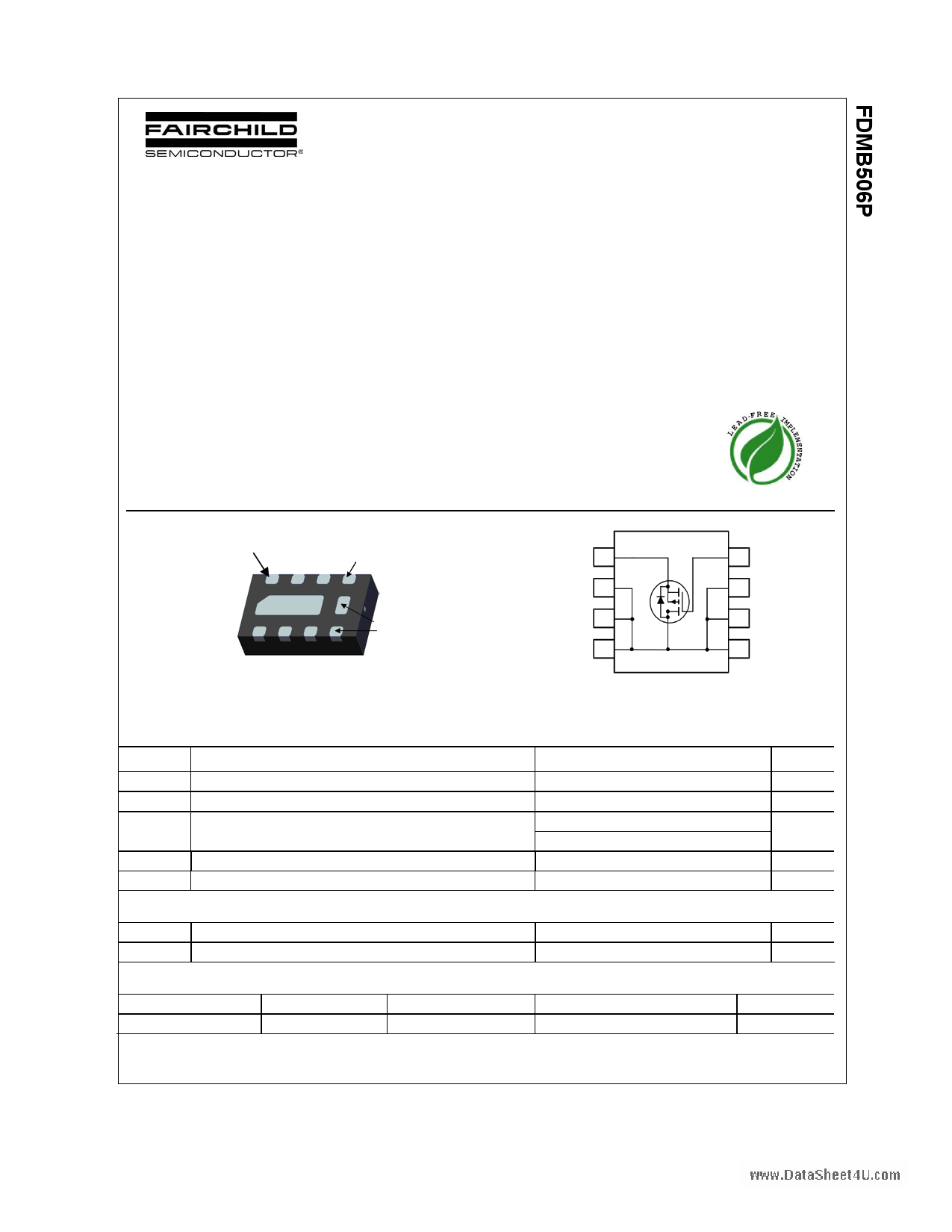
PIN 1
GATE
SOURCE
www.DataSheet4U.com
MicroFET
3x1.9
Absolute Maximum Ratings TA=25oC unless otherwise noted
Symbol
Parameter
VDSS
VGSS
ID
Drain-Source Voltage
Gate-Source Voltage
Drain Current – Continuous
– Pulsed
(Note 1a)
PD Power Dissipation
(Note 1a)
TJ, TSTG
Operating and Storage Junction Temperature Range
Thermal Characteristics
RθJA Thermal Resistance, Junction-to-Ambient
RθJA Thermal Resistance, Junction-to-Ambient
(Note 1a)
(Note 1b)
Package Marking and Ordering Information
Device Marking
Device
Reel Size
506 FDMB506P
7’’
S5
D6
D7
D8
4G
3D
2D
1D
Ratings
–20
±8
–6.8
70
1.9
–55 to +150
65
208
Tape width
8mm
Units
V
V
A
W
°C
°C/W
Quantity
3000 units
2005 Fairchild Semiconductor Corporation
FDMB506P Rev C1(W)
1 page 
Typical Characteristics
5
ID = -6.8A
4
3
VDS = -5V
-10V
-15V
2
1
0
0 5 10 15 20 25
Qg, GATE CHARGE (nC)
Figure 7. Gate Charge Characteristics.
100
RDS(ON) LIMIT
10
1
VGS = -4.5V
0.1 SINGLE PULSE
RθJA = 160oC/W
TA = 25oC
100µs
1ms
10ms
100ms
1s
10s
DC
0.01
0.1
1 10
-VDS, DRAIN-SOURCE VOLTAGE (V)
100
Figure 9. Maximum Safe Operating Area.
3200
2800
2400
CISS
f = 1 MHz
VGS = 0 V
2000
1600
1200
800
COSS
400
CRSS
0
0
5 10 15
-VDS, DRAIN TO SOURCE VOLTAGE (V)
20
Figure 8. Capacitance Characteristics.
10
SINGLE PULSE
8 RθJA = 160°C/W
TA = 25°C
6
4
2
0
0.01
0.1
1 10
t1, TIME (sec)
100
Figure 10. Single Pulse Maximum
Power Dissipation.
1000
1
0.1
0.01
D = 0.5
0.2
0.1
0.05
0.02
0.01
0.001
0.0001
SINGLE PULSE
0.001
0.01
0.1
t1, TIME (sec)
1
RθJA(t) = r(t) * RθJA
RθJA = 160oC/W
P(pk)
t1
t2
TJ - TA = P * RθJA(t)
Duty Cycle, D = t1 / t2
10 100 1000
Figure 9. Transient Thermal Response Curve.
Thermal characterization performed using the conditions described in Note 1c.
Transient thermal response will change depending on the circuit board design.
FDMB506P Rev C1(W)
5 Page | ||
| Páginas | Total 6 Páginas | |
| PDF Descargar | [ Datasheet FDMB506P.PDF ] | |
Hoja de datos destacado
| Número de pieza | Descripción | Fabricantes |
| FDMB506P | P-Channel 1.8V Logic Level PowerTrench MOSFET | Fairchild Semiconductor |
| Número de pieza | Descripción | Fabricantes |
| SLA6805M | High Voltage 3 phase Motor Driver IC. |
Sanken |
| SDC1742 | 12- and 14-Bit Hybrid Synchro / Resolver-to-Digital Converters. |
Analog Devices |
|
DataSheet.es es una pagina web que funciona como un repositorio de manuales o hoja de datos de muchos de los productos más populares, |
| DataSheet.es | 2020 | Privacy Policy | Contacto | Buscar |