|
|
|
PDF ZL50075 Data sheet ( Hoja de datos )
| Número de pieza | ZL50075 | |
| Descripción | 32 K Channel Digital Switch | |
| Fabricantes | Zarlink Semiconductor | |
| Logotipo | ||
Hay una vista previa y un enlace de descarga de ZL50075 (archivo pdf) en la parte inferior de esta página. Total 30 Páginas | ||
|
No Preview Available !
ZL50075
32 K Channel Digital Switch with High Jitter
Tolerance, Rate Conversion per Group of
2 Streams (8, 16, 32 or 64 Mbps),
and 64 Inputs and 64 Outputs
Data Sheet
Features
January 2006
• 32,768 channel x 32,768 channel non-blocking
digital Time Division Multiplex (TDM) switch at
65.536 Mbps or 32.768 Mbps or using a
combination of rates
• 16,384 channel x 16,384 channel non-blocking
digital TDM switch at 16.384 Mbps
Ordering Information
ZL50075GAC 324 Ball PBGA Trays
ZL50075GAG2 324 Ball PBGA** Trays
**Pb Free Tin/Silver/Copper
-40°C to +85°C
• 8,192 channel x 8,192 channel non-blocking
digital TDM switch at 8.192 Mbps
• Per-channel A-Law/µ-Law Translation
• High jitter tolerance with multiple input clock
sources and frequencies
• Per-channel constant or variable throughput delay
for frame integrity and low latency applications
• Up to 64 serial TDM input streams, divided into
• Per-stream Bit Error Rate (BER) test circuits
32 groups with 2 input streams per group
• Per-channel high impedance output control
• Up to 64 serial TDM output streams, divided into
32 groups with 2 output streams per group
• Per-group input and output data rate conversion
selection at 65.536 Mbps, 32.768 Mbps,
16.384 Mbps and 8.192 Mbps. Input and output
data group rates can differ
• Per-channel force high output control
• Per-channel message mode
• Control interface compatible with Intel and
Motorola 16 bit non-multiplexed buses
• Connection memory block programming
•
Per-group input
point selection
bit
delay
for
flexible
sampling
• Supports
input andwww.DataSheet4U.com
ST-BUS and GCI-Bus
output timing
standards
for
• Per-group output fractional bit advancement
• IEEE 1149.1 (JTAG) test port
• Two sets of output timing signals for interfacing
additional devices
• 3.3 V I/O with 5V tolerant inputs; 1.8 V core
voltage
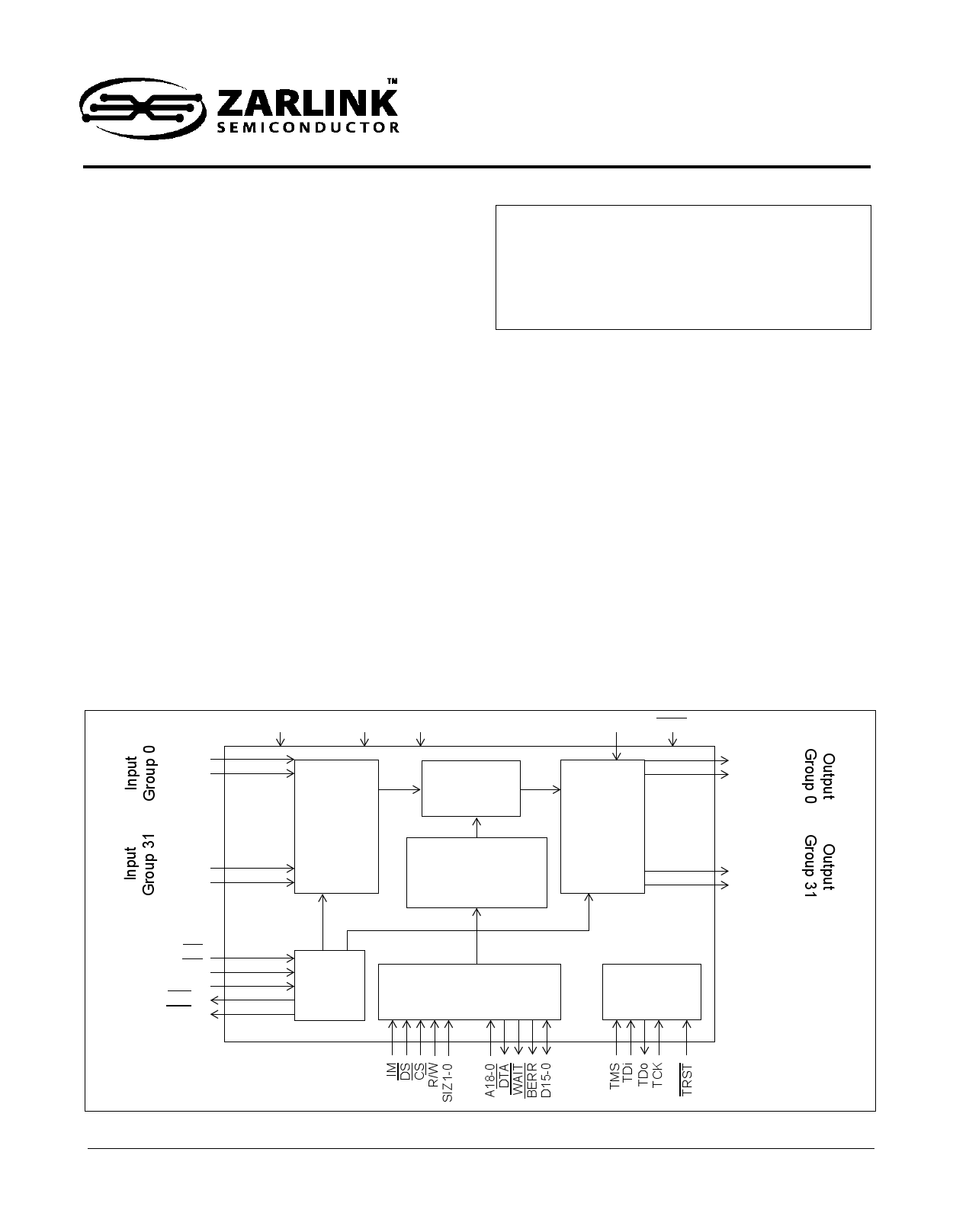
STiA0
STiB0
:
:
STiA31
STiB31
FPi0
CKi0
CK_SEL1-0
FPo1-0
CKo1-0
VDD_CORE VDD_IO VSS
ODE PWR
S/P
Converter
Input
Timing
Data Memory
P/S
Converter
Connection Memory
Output
Timing
Timing
Microprocessor Interface
and Control Registers
Test Access
Port
SToA0
SToB0
:
:
SToA31
SToB31
Figure 1 - ZL50075 Functional Block Diagram
1
Zarlink Semiconductor Inc.
Zarlink, ZL and the Zarlink Semiconductor logo are trademarks of Zarlink Semiconductor Inc.
Copyright 2004-2006, Zarlink Semiconductor Inc. All Rights Reserved.
1 page 
ZL50075
Data Sheet
List of Figures
Figure 1 - ZL50075 Functional Block Diagram . . . . . . . . . . . . . . . . . . . . . . . . . . . . . . . . . . . . . . . . . . . . . . . . . . . . 1
Figure 2 - 32 K x 32 K Channel Basic Switch Configuration . . . . . . . . . . . . . . . . . . . . . . . . . . . . . . . . . . . . . . . . . 14
Figure 3 - Input and Output Data Rate Conversion Example. . . . . . . . . . . . . . . . . . . . . . . . . . . . . . . . . . . . . . . . . 16
Figure 4 - Input Sampling Point Delay Programming. . . . . . . . . . . . . . . . . . . . . . . . . . . . . . . . . . . . . . . . . . . . . . . 18
Figure 5 - Output Bit Advancement Timing . . . . . . . . . . . . . . . . . . . . . . . . . . . . . . . . . . . . . . . . . . . . . . . . . . . . . . 19
Figure 6 - Data Throughput Delay for Constant Delay. . . . . . . . . . . . . . . . . . . . . . . . . . . . . . . . . . . . . . . . . . . . . . 21
Figure 7 - Data Throughput Delay for Variable Delay . . . . . . . . . . . . . . . . . . . . . . . . . . . . . . . . . . . . . . . . . . . . . . 21
Figure 8 - Example PRBS Timeslot Insertion. . . . . . . . . . . . . . . . . . . . . . . . . . . . . . . . . . . . . . . . . . . . . . . . . . . . . 23
Figure 9 - Read Cycle Operation . . . . . . . . . . . . . . . . . . . . . . . . . . . . . . . . . . . . . . . . . . . . . . . . . . . . . . . . . . . . . . 26
Figure 10 - Write Cycle Operation . . . . . . . . . . . . . . . . . . . . . . . . . . . . . . . . . . . . . . . . . . . . . . . . . . . . . . . . . . . . . 27
Figure 11 - Frame Pulse Input and Clock Input . . . . . . . . . . . . . . . . . . . . . . . . . . . . . . . . . . . . . . . . . . . . . . . . . . . 49
Figure 12 - ST-Bus Frame Pulse and Clock Output Timing . . . . . . . . . . . . . . . . . . . . . . . . . . . . . . . . . . . . . . . . . . 51
Figure 13 - GCI Frame Pulse and Clock Output Timing . . . . . . . . . . . . . . . . . . . . . . . . . . . . . . . . . . . . . . . . . . . . 51
Figure 14 - Serial Data Timing to CKi . . . . . . . . . . . . . . . . . . . . . . . . . . . . . . . . . . . . . . . . . . . . . . . . . . . . . . . . . . 53
Figure 15 - Serial Data Timing to CKo . . . . . . . . . . . . . . . . . . . . . . . . . . . . . . . . . . . . . . . . . . . . . . . . . . . . . . . . . . 55
Figure 16 - Microprocessor Bus Interface Timing . . . . . . . . . . . . . . . . . . . . . . . . . . . . . . . . . . . . . . . . . . . . . . . . . 57
Figure 17 - Intel Mode Timing . . . . . . . . . . . . . . . . . . . . . . . . . . . . . . . . . . . . . . . . . . . . . . . . . . . . . . . . . . . . . . . . 57
Figure 18 - IEEE 1149.1 Test Port & PWR Reset Timing. . . . . . . . . . . . . . . . . . . . . . . . . . . . . . . . . . . . . . . . . . . . 58
5
Zarlink Semiconductor Inc.
5 Page 
Pin Description (continued)
Pin
B14
A16
A15
A18
C12
C13
B15, B18
B2
B16
ZL50075
Data Sheet
Name
CS
DS
R/W
DTA
BERR
WAIT
SIZ0-1
IM
PWR
Description
Chip Select Input (5 V Tolerant Input)
Active low input used with DS to enable read and write access to
the ZL50075.
Data Strobe Input (5 V Tolerant Input)
Active low input used with CS to enable read and write access to
the ZL50075.
Read/Write Input (5 V Tolerant Input)
Input signal that controls the type of microprocessor access:
0 - Microprocessor write to the ZL50075
1 - Microprocessor read from the ZL50075
Data Transfer Acknowledge (5 V Tolerant, 3.3 V Tri-state Output
with Slew-Rate)
Active low output which indicates that a data bus transfer is
complete. An external pull-up resistor is required to hold this pin
HIGH when output is high-impedance.
Transfer Bus Error Output with Slew Rate Control (5 V Tolerant,
3.3 V Tri-state Outputs with Slew-Rate Control)
This pin goes low whenever the microprocessor attempts to access
an invalid memory space inside the device. In Motorola bus mode, if
this bus error signal is activated, the data transfer acknowledge
signal, DTA, will not be generated. In Intel bus mode, the generation
of the DTA is not affected by this BERR signal. An external pull-up
resistor is required to hold a HIGH level when output is
high-impedance.
Data Transfer Wait Output (5 V Tolerant, 3.3 V Tri-state Output
with Slew Rate)
Active low wait signal output. An external pull-up resistor is required
to hold a HIGH level when output is high-impedance.
Data Transfer Size/Upper and Lower Data Strobe Inputs (5 V
Tolerant Inputs)
Motorola mode: SIZ0 - LDS, SIZ1 - UDS.
Active low upper and lower data strobes, UDS and LDS, indicate
whether the upper byte, D15-8, and/or lower byte, D7-0, is being
transferred.
Intel mode: SIZ0 - BE0, SIZ1 - BE1.
Active low Intel type bus-enable signal BE1 and BE0 signals
Microprocessor Port Bus Mode Select (5 V Tolerant Input)
Control input:
0 = Motorola mode
1 = Intel mode
Device Reset (5 V Tolerant Schmitt-Triggered Input)
Asynchronous reset input used to initialize the ZL50075.
0 = Reset
1 = Normal
See Section 11.0, Power-up and Initialization of the ZL50075 for
detailed description of Reset state.
11
Zarlink Semiconductor Inc.
11 Page | ||
| Páginas | Total 30 Páginas | |
| PDF Descargar | [ Datasheet ZL50075.PDF ] | |
Hoja de datos destacado
| Número de pieza | Descripción | Fabricantes |
| ZL50070 | 24 K Channel Digital Switch | Zarlink Semiconductor |
| ZL50073 | 32 K Channel Digital Switch | Zarlink Semiconductor |
| ZL50074 | 32 K x 32 K Channel TDM Switch | Zarlink Semiconductor |
| ZL50075 | 32 K Channel Digital Switch | Zarlink Semiconductor |
| Número de pieza | Descripción | Fabricantes |
| SLA6805M | High Voltage 3 phase Motor Driver IC. |
Sanken |
| SDC1742 | 12- and 14-Bit Hybrid Synchro / Resolver-to-Digital Converters. |
Analog Devices |
|
DataSheet.es es una pagina web que funciona como un repositorio de manuales o hoja de datos de muchos de los productos más populares, |
| DataSheet.es | 2020 | Privacy Policy | Contacto | Buscar |