|
|
|
PDF UR5512 Data sheet ( Hoja de datos )
| Número de pieza | UR5512 | |
| Descripción | 2A DDR BUS TERMINATION REGULATOR | |
| Fabricantes | Unisonic Technologies | |
| Logotipo | ||
Hay una vista previa y un enlace de descarga de UR5512 (archivo pdf) en la parte inferior de esta página. Total 7 Páginas | ||
|
No Preview Available !
www.DataSheet4U.com
UNISONIC TECHNOLOGIES CO., LTD
UR5512
LINEAR INTEGRATED CIRCUIT
2A DDR BUS TERMINATION
REGULATOR
DESCRIPTION
The UR5512 is a linear regulator which provides up to 2 Amp
bi-directional driving and sinking capability for DDR SDRAM bus
terminator application. The output termination voltage tracks the
reference voltage applied at VREF pin. A resistor divider connected to
VIN, GND and VREF pins is used to force a reference voltage to VREF
pin.
The UR5512 contains a high-speed operational amplifier to
provide excellent response to line/load transient. An active-low
shutdown (VREF) pin provides Suspend to RAM (STR) functionality.
Additional features include current limiting protection, on-chip
thermal shut-down protection.
FEATURES
* DDR-II Termination Voltage applications
* Driving and sinking current up to 2A
* Low output voltage offset (within 20mV@±2A)
* Adjustable output voltage by external resistors
* Suspend to RAM (STR) functionality
* Current limiting protection
* Thermal protection
* Cost-effective and easy to use
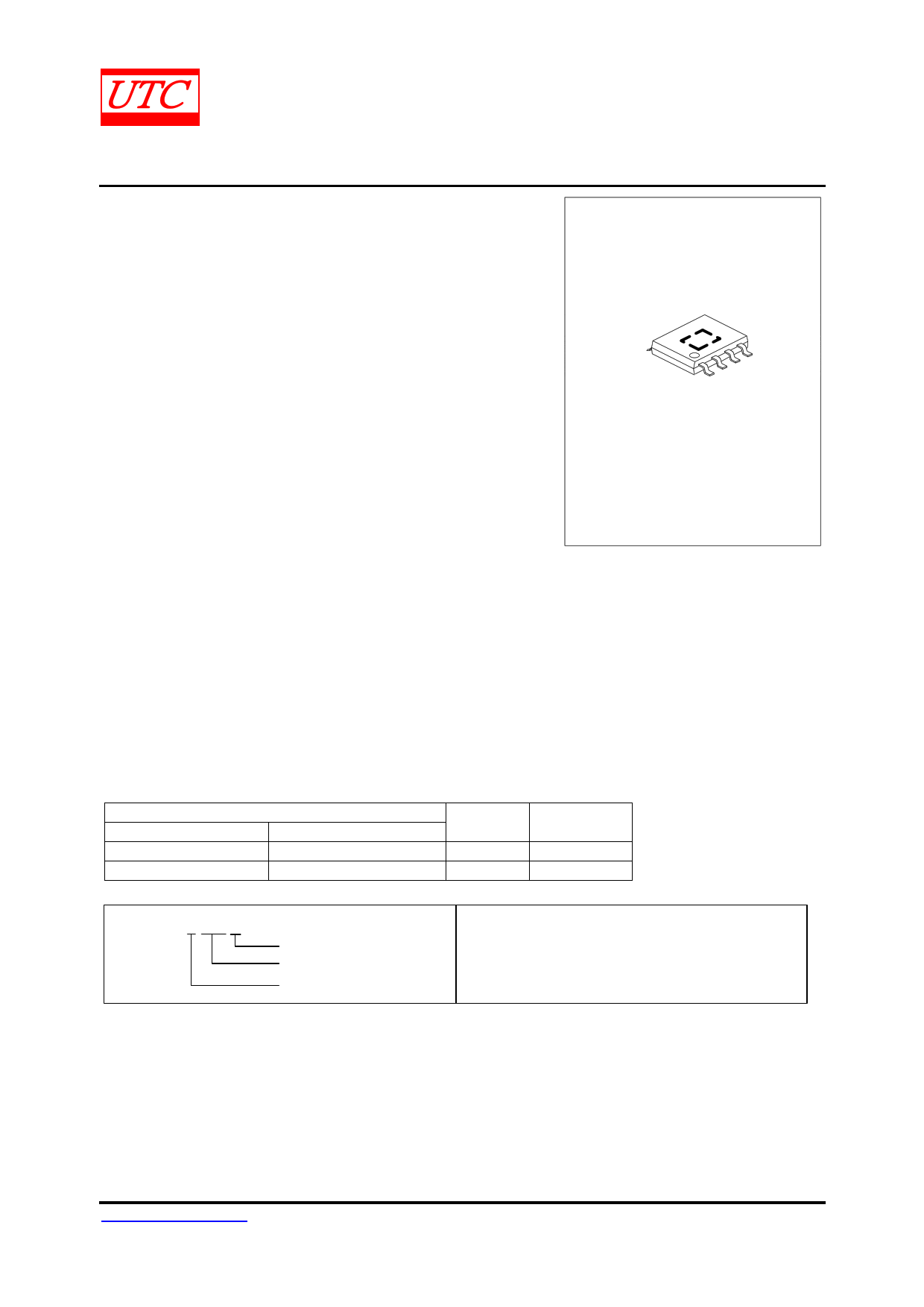
HSOP -8
*Pb-free plating product number: UR5512L
ORDERING INFORMATION
Order Number
Normal
Lead Free Plating
UR5512-SH2-R
UR5512L-SH2-R
UR5512-SH2-T
UR5512L-SH2-T
UR5512L-SH2-R
(1)Packing Type
(2)Package Type
(3)Lead Plating
Package
HSOP-8
HSOP-8
Packing
Tape Reel
Tube
(1) R: Tape Reel, T: Tube
(2) SH2: HSOP-8
(3) L: Lead Free Plating, Blank: Pb/Sn
www.unisonic.com.tw
Copyright © 2005 Unisonic Technologies Co., Ltd
1 of 7
QW-R101-017,A
1 page 
UR5512
FUNCTIONAL DESCRIPTION
LINEAR INTEGRATED CIRCUIT
General Information
The UR5512 is a linear regulator designed for DDR SDRAM bus terminator application. The output, VOUT is
capable of sourcing or sinking current up to 2A peak while regulating the output voltage to within 20mV offset. The
UR5512 has excellent response to load regulation while preventing shoot through. Active-low shutdown mechanism
and fault protections. The UR5512 is available in several packages to meet different power dissipation and surface
mount applications.
Output Voltage Regulation
The output voltage tracks the reference voltage applied at VREF pin. Two internal NPN pass transistors act as the
buffered output regulate the output voltage by sourcing current from VIN pin or sinking current to GND pin. An internal
Kelvin sensing scheme is use at the VOUT pin to improve load regulation at various load current. Since the UR5512
exhibits excellent response to load transient, lesser amount of capacitors can be used.
Current Limit
An internal current limiting sensor is used to monitor the maximum output current to prevent damages from
overload or short-circuit condition. Increasing the input voltage of VIN or VCNTL will get higher current-limit points.
Shutdown and Soft-Start
An additional function of the VREF pin is acting as a shutdown control input that can be used for suspend to RAM
functionality. Applying and holding a voltage below 0.15V to VREF pin shuts down the output of the regulator. An
external NPN transistor or N-channel MOSFET is used to pull down the VREF pin voltage; while applying a “high”
signal to turn on the transistor. During shutdown condition, the two pass transistors are turned off and the output
VOUT will tri-state; sourcing or sinking no current. When releasing the VREF pin, the current through the resistor divider
charges the capacitor Css to initiate a soft-start cycle.
Thermal Shutdown
If the junction temperature exceeds the thermal shutdown (TJ= +150°C) then the part will enter a shutdown state.
A thermal sensor turns off both pass transistors, allowing the device to cool down. After the junction temperature
reduces by 40°C, the regulator starts to regulate again; resulting in a pulsed output during continuous thermal
overload conditions.
Power Inputs
Input power up sequence are not required for VIN and VCNTL. Be careful; do not apply voltage to VOUT when there is
no VCNTL voltage presented. This is due to the internal parasitic diodes between VOUT to VIN and VOUT to VCNTL which
will be forward bias.
Reference Voltage
The reference voltage is programmed by a resistor divider between VIN and GND pins. The recommended resistor
is < 5kΩ to maintain the accuracy of the output voltage. For improved the performance, an external bypass capacitor
can be used, located close to VREF pin to help with noise. A ceramic capacitor can be use and is selected to be
greater than 0.1µF. Do not place any additional loading on this reference input pin.
UNISONIC TECHNOLOGIES CO., LTD
www.unisonic.com.tw
5 of 7
QW-R101-017,A
5 Page | ||
| Páginas | Total 7 Páginas | |
| PDF Descargar | [ Datasheet UR5512.PDF ] | |
Hoja de datos destacado
| Número de pieza | Descripción | Fabricantes |
| UR5512 | 2A DDR BUS TERMINATION REGULATOR | Unisonic Technologies |
| UR5515 | 1.5A/3A BUS TERMINATION REGULATOR | Unisonic Technologies |
| UR5516 | 3A BUS TERMINATION REGULATOR | Unisonic Technologies |
| Número de pieza | Descripción | Fabricantes |
| SLA6805M | High Voltage 3 phase Motor Driver IC. |
Sanken |
| SDC1742 | 12- and 14-Bit Hybrid Synchro / Resolver-to-Digital Converters. |
Analog Devices |
|
DataSheet.es es una pagina web que funciona como un repositorio de manuales o hoja de datos de muchos de los productos más populares, |
| DataSheet.es | 2020 | Privacy Policy | Contacto | Buscar |