|
|
|
PDF MAX1518B Data sheet ( Hoja de datos )
| Número de pieza | MAX1518B | |
| Descripción | TFT-LCD DC-DC Converter | |
| Fabricantes | Maxim Integrated Products | |
| Logotipo | ||
1. MAX1518B Hay una vista previa y un enlace de descarga de MAX1518B (archivo pdf) en la parte inferior de esta página. Total 25 Páginas | ||
|
No Preview Available !
MAX1518B
EVALUATION KIT AVAILABLE
TFT-LCD DC-DC Converter with
Operational Amplifiers
General Description
The MAX1518B includes a high-performance step-up
regulator, two linear-regulator controllers, and high-current
operational amplifiers for active-matrix, thin-film transistor
(TFT), liquid-crystal displays (LCDs). Also included is a
logic-controlled, high-voltage switch with adjustable delay.
The step-up DC-DC converter provides the regulated
supply voltage for the panel source driver ICs. The
converter is a high-frequency (1.2MHz) current-mode
regulator with an integrated 14V n-channel MOSFET
that allows the use of ultra-small inductors and ceramic
capacitors. It provides fast transient response to pulsed
loads while achieving efficiencies over 85%.
The gate-on and gate-off linear-regulator controllers
provide regulated TFT gate-on and gate-off supplies using
external charge pumps attached to the switching node. The
MAX1518B includes five high-performance operational
amplifiers. These amplifiers are designed to drive the LCD
backplane (VCOM) and/or the gamma-correction divider
string. The device features high output current (±150mA),
fast slew rate (13V/μs), wide bandwidth (12MHz), and
rail-to-rail inputs and outputs.
The MAX1518B is available in a 32-pin thin QFN package
with a maximum thickness of 0.8mm for ultra-thin LCD
panels.
Applications
●● Notebook Computer Displays
●● LCD Monitor Panels
Ordering Information
PART
TEMP RANGE
MAX1518BETJ
-40°C to +100°C
PIN-PACKAGE
32 Thin QFN
(5mm x 5mm)
Pin Configuration appears at end of data sheet.
Features
●● 2.6V to 6.5V Input Supply Range
●● 1.2MHz Current-Mode Step-Up Regulator
• Fast Transient Response to Pulsed Load
• High-Accuracy Output Voltage (1.5%)
• Built-In 14V, 2.4A, 0.16Ω n-Channel MOSFET
• High Efficiency (90%)
●● Linear-Regulator Controllers for VGON and VGOFF
●● High-Performance Operational Amplifiers
• ±150mA Output Short-Circuit Current
• 13V/μs Slew Rate
• 12MHz, -3dB Bandwidth
• Rail-to-Rail Inputs/Outputs
●● Logic-Controlled, High-Voltage Switch with
Adjustable Delay
●● Timer-Delay Fault Latch for All Regulator Outputs
●● Thermal-Overload Protection
●● 0.6mA Quiescent Current
Minimal Operating Circuit
VCN VCP
VIN
IN
STEP-UP
CONTROLLER
LX
FB
COMP
MAX1518B
GATE-ON
CONTROLLER
PGND
AGND
DRVP
FBP
SRC
COM
DRN
SWITCH
CONTROL
SUP
NEG1
GATE-OFF
CONTROLLER
OUT1
POS1
NEG2
OP1
REF
DEL
CTL
DRVN
FBN
REF
NEG4
OUT2
POS2
OP2
OP4 OUT4
POS4
NEG5
OUT3
POS3
OP3
OP5 OUT5
BGND
POS5
VMAIN
VCP
VGON
VCN
VGOFF
19-3244; Rev 1; 11/14
1 page 
MAX1518B
TFT-LCD DC-DC Converter with
Operational Amplifiers
Electrical Characteristics (continued)
(VIN = 3V, VSUP = 8V, PGND = AGND = BGND = 0, IREF = 25μA, TA = 0°C to +85°C. Typical values are at TA = +25°C, unless
otherwise noted.)
PARAMETER
IN Supply Range
IN Undervoltage-Lockout
Threshold
IN Quiescent Current
REF Output Voltage
MAIN STEP-UP REGULATOR
Output Voltage Range
Operating Frequency
FB Regulation Voltage
FB Line Regulation
FB Input Bias Current
FB Transconductance
LX On-Resistance
LX Current Limit
OPERATIONAL AMPLIFIERS
SUP Supply Range
SUP Supply Current
Input Offset Voltage
Input Common-Mode Range
SYMBOL
VIN
CONDITIONS
VUVLO VIN rising, typical hysteresis = 150mV
VFB = VFBP = 1.4V, VFBN = 0,
LX not switching
IIN VFB = 1.1V, VFBP = 1.4V, VFBN = 0,
LX switching
-2µA < IREF < 50µA, VIN = 2.6V to 5.5V
VMAIN
fOSC
VFB
RLX(ON)
ILIM
No load
VIN = 2.6V to 5.5V
VFB = 1.4V
∆ICOMP = 5µA
VFB = 1V, duty cycle = 65%
VSUP
ISUP
VOS
VCM
Buffer configuration, VPOS_ = 4V, no load
(VNEG_, VPOS_, VOUT_) @ VSUP/2
Output Voltage Swing, High
VOH
IOUT_ = 100µA
IOUT_ = 5mA
Output Voltage Swing, Low
Short-Circuit Current
VOL
IOUT_ = -100µA
IOUT_ = -5mA
To VSUP/2
Source
Sink
Output Source-and-Sink Current
(VNEG_ , VPOS_, VOUT_) @ VSUP/2,
|∆VOS| < 10mV (|VOS| < 30mV for OUT3)
GATE-ON LINEAR-REGULATOR CONTROLLER
FBP Regulation Voltage
FBP Effective Load-Regulation
Error (Transconductance)
VFBP
IDRVP = 100µA
VDRVP = 10V, IDRVP = 50µA to 1mA
FBP Line (IN) Regulation Error
DRVP Sink Current
IDRVP
IDRVP = 100µA, 2.6V < VIN < 5.5V
VFBP = 1.1V, VDRVP = 10V
MIN TYP MAX UNITS
2.6 5.5 V
2.250
2.715
V
0.8 mA
1.222
11
1.269
V
VIN
1020
1.212
-40
75
2.5
13
1380
1.250
±0.15
+40
300
250
3.5
V
kHz
V
%/ V
nA
µS
mΩ
A
4.5
0
VSUP
-15
VSUP
-150
50
50
40
13.0
3.8
12
VSUP
V
mA
mV
V
mV
15
mV
150
mA
mA
1.218
1
1.269
-2
5
V
%
mV
mA
www.maximintegrated.com
Maxim Integrated │ 5
5 Page 
MAX1518B
TFT-LCD DC-DC Converter with
Operational Amplifiers
Typical Operating Circuit
The MAX1518B Typical Operating Circuit (Figure 1) is a
complete power-supply system for TFT LCDs. The circuit
generates a +13V source-driver supply and +24V and -8V
gate-driver supplies. The input voltage range for the IC is
from +2.6V to +6.5V. The listed load currents in Figure 1
are available from a +4.5V to +5.5V supply. Table 1 lists
some recommended components, and Table 2 lists the
contact information of component suppliers.
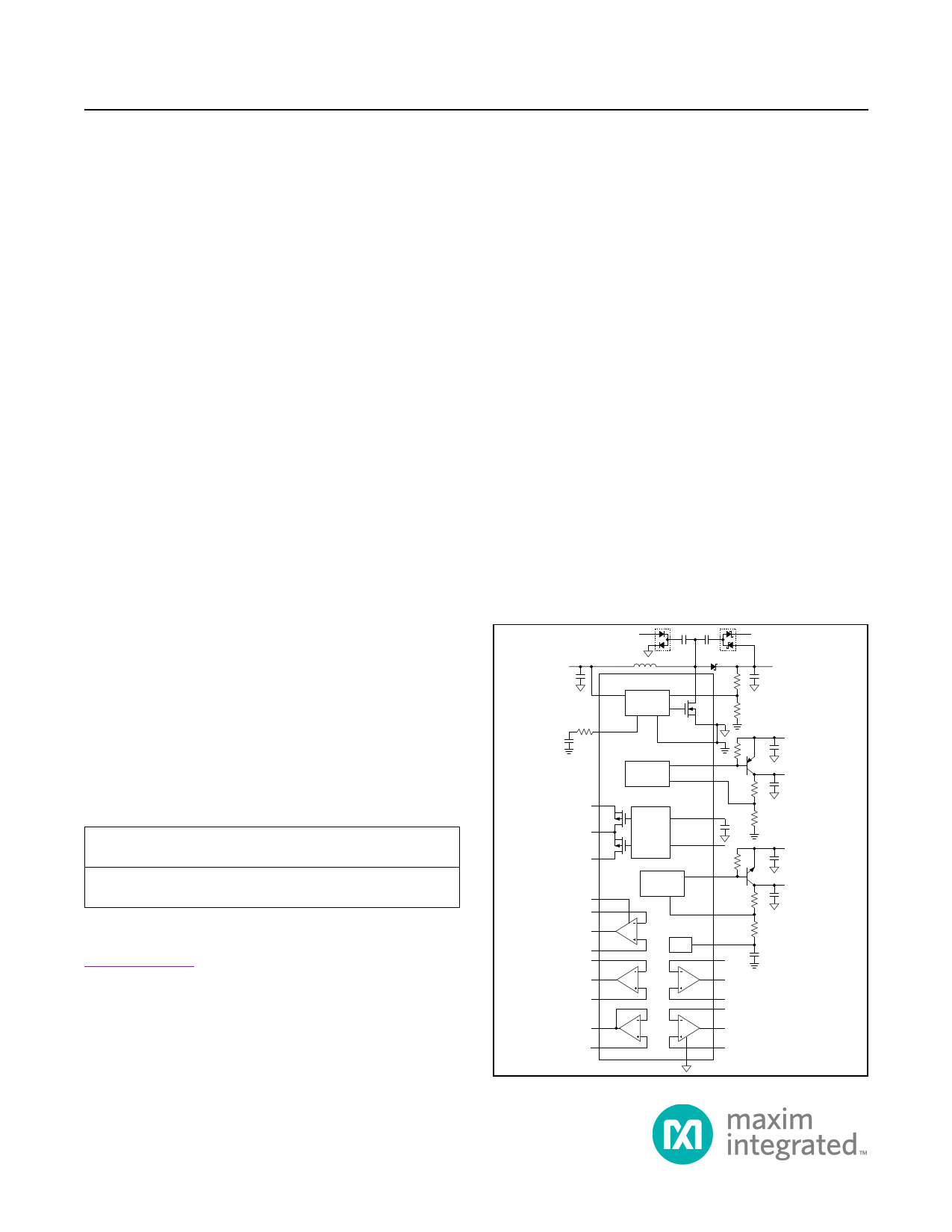
Detailed Description
The MAX1518B contains a high-performance step-
up switching regulator, two low-cost linear-regulator
controllers, multiple high-current operational amplifiers,
and startup timing and level-shifting functionality useful for
active-matrix TFT LCDs. Figure 2 shows the MAX1518B
Functional Diagram.
Main Step-Up Regulator
The main step-up regulator employs a current-mode,
fixed-frequency PWM architecture to maximize loop band-
width and provide fast transient response to pulsed loads
typical of TFT-LCD panel source drivers. The 1.2MHz
switching frequency allows the use of low-profile inductors
and ceramic capacitors to minimize the thickness of LCD
panel designs. The integrated high-efficiency MOSFET
and the IC’s built-in digital soft-start functions reduce the
number of external components required while controlling
inrush currents. The output voltage can be set from VIN to
13V with an external resistive voltage-divider. To generate
an output voltage greater than 13V, an external cascoded
MOSFET is needed. See the Generating Output Voltages
> 13V section in the Design Procedures.
The regulator controls the output voltage and the power
delivered to the output by modulating the duty cycle (D) of
the internal power MOSFET in each switching cycle. The
duty cycle of the MOSFET is approximated by:
D ≈ VMAIN − VIN
VMAIN
Table 1. Component List
DESIGNATION
DESCRIPTION
C1
22µF, 6.3V X5R ceramic capacitor (1210)
TDK C3225X5R0J227M
C2
22µF, 16V X5R ceramic capacitor (1812)
TDK C4532X5X1C226M
D1
3A, 30V Schottky diode (M-flat)
Toshiba CMS02
D2, D3
200mA, 100V, dual ultra-fast diodes (SOT23)
Fairchild MMBD4148SE
L1
3.0µH, 3A inductor
Sumida CDRH6D28-3R0
Q1
200mA, 40V pnp bipolar transistor (SOT23)
Fairchild MMBT3906
Q2
200mA, 40V npn bipolar transistor (SOT23)
Fairchild MMBT3904
Figure 3 shows the Functional Diagram of the step-up
regulator. An error amplifier compares the signal at FB
to 1.236V and changes the COMP output. The voltage at
COMP sets the peak inductor current. As the load varies,
the error amplifier sources or sinks current to the COMP
output accordingly to produce the inductor peak current
necessary to service the load. To maintain stability at high
duty cycles, a slope-compensation signal is summed with
the current-sense signal.
On the rising edge of the internal clock, the controller
sets a flip-flop, turning on the n-channel MOSFET and
applying the input voltage across the inductor. The current
through the inductor ramps up linearly, storing energy in
its magnetic field. Once the sum of the current-feedback
signal and the slope compensation exceeds the COMP
voltage, the controller resets the flip-flop and turns off
the MOSFET. Since the inductor current is continuous,
a transverse potential develops across the inductor that
turns on the diode (D1). The voltage across the inductor
then becomes the difference between the output voltage
and the input voltage.
Table 2. Component Suppliers
SUPPLIER
Fairchild
Sumida
TDK
Toshiba
PHONE
408-822-2000
847-545-6700
847-803-6100
949-455-2000
FAX
408-822-2102
847-545-6720
847-390-4405
949-859-3963
WEBSITE
www.fairchildsemi.com
www.sumida.com
www.component.tdk.com
www.toshiba.com/taec
www.maximintegrated.com
Maxim Integrated │ 11
11 Page | ||
| Páginas | Total 25 Páginas | |
| PDF Descargar | [ Datasheet MAX1518B.PDF ] | |
Hoja de datos destacado
| Número de pieza | Descripción | Fabricantes |
| MAX1518 | (MAX1516 - MAX1518) TFT-LCD DC-DC Converters | Maxim Integrated Products |
| MAX1518A | TFT-LCD DC-DC Converters | Maxim Integrated |
| MAX1518B | TFT-LCD DC-DC Converter | Maxim Integrated Products |
| Número de pieza | Descripción | Fabricantes |
| SLA6805M | High Voltage 3 phase Motor Driver IC. |
Sanken |
| SDC1742 | 12- and 14-Bit Hybrid Synchro / Resolver-to-Digital Converters. |
Analog Devices |
|
DataSheet.es es una pagina web que funciona como un repositorio de manuales o hoja de datos de muchos de los productos más populares, |
| DataSheet.es | 2020 | Privacy Policy | Contacto | Buscar |