|
|
|
PDF ZL30227 Data sheet ( Hoja de datos )
| Número de pieza | ZL30227 | |
| Descripción | (ZL30226 - ZL30228) 4/8/16 Port IMA/TC PHY Device | |
| Fabricantes | Zarlink Semiconductor | |
| Logotipo | ||
Hay una vista previa y un enlace de descarga de ZL30227 (archivo pdf) en la parte inferior de esta página. Total 30 Páginas | ||
|
No Preview Available !
www.DataSheet4U.com
ZL30226/7/8
4/8/16 Port IMA/TC PHY Device for xDSL
Data Sheet
Features
IMA
• Up to 16 xDSL links & up to 8 IMA groups with 1
to 16 links/IMA group1
• Supports symmetrical & asymmetrical operation
• CTC (common transmit) & ITC (independent
transmit) clocking modes
• Pre-processing of RX ICP (IMA control protocol)
cells
• IMA layer & per link statistics and alarms for
performance monitoring with MIB support
TC and UNI
• Supports mixed-mode operation: links not
assigned to an IMA group can be used in TC
mode
• ATM framing using cell delineation
1. ZL30226 supports up to 4 serial links with maximum 4 groups
to be used - groups 0, 1, 2, 3.
ZL30227 supports up to 8 serial links
ZL30228 supports up to 16 serial links
March 2004
Ordering Information
ZL30226/GA 384 Pin PBGA
ZL30227/GA 384 Pin PBGA
ZL30228/GA 384 Pin PBGA
-40°C to +85°C
• HEC (header error control) verification &
generation, error detection, filler cell filtering
(IMA) and idle/unassigned cell filtering (TC)
• TC layer statistics and error counts i.e. HEC
errors with MIB support
Standards Compliant
• ATM Forum - IMA 1.1 (AF-PHY-0086.001) &
backwards compatible with IMA 1.0
• ITU G.804 cell mapping & ITU I.432 cell
delineation
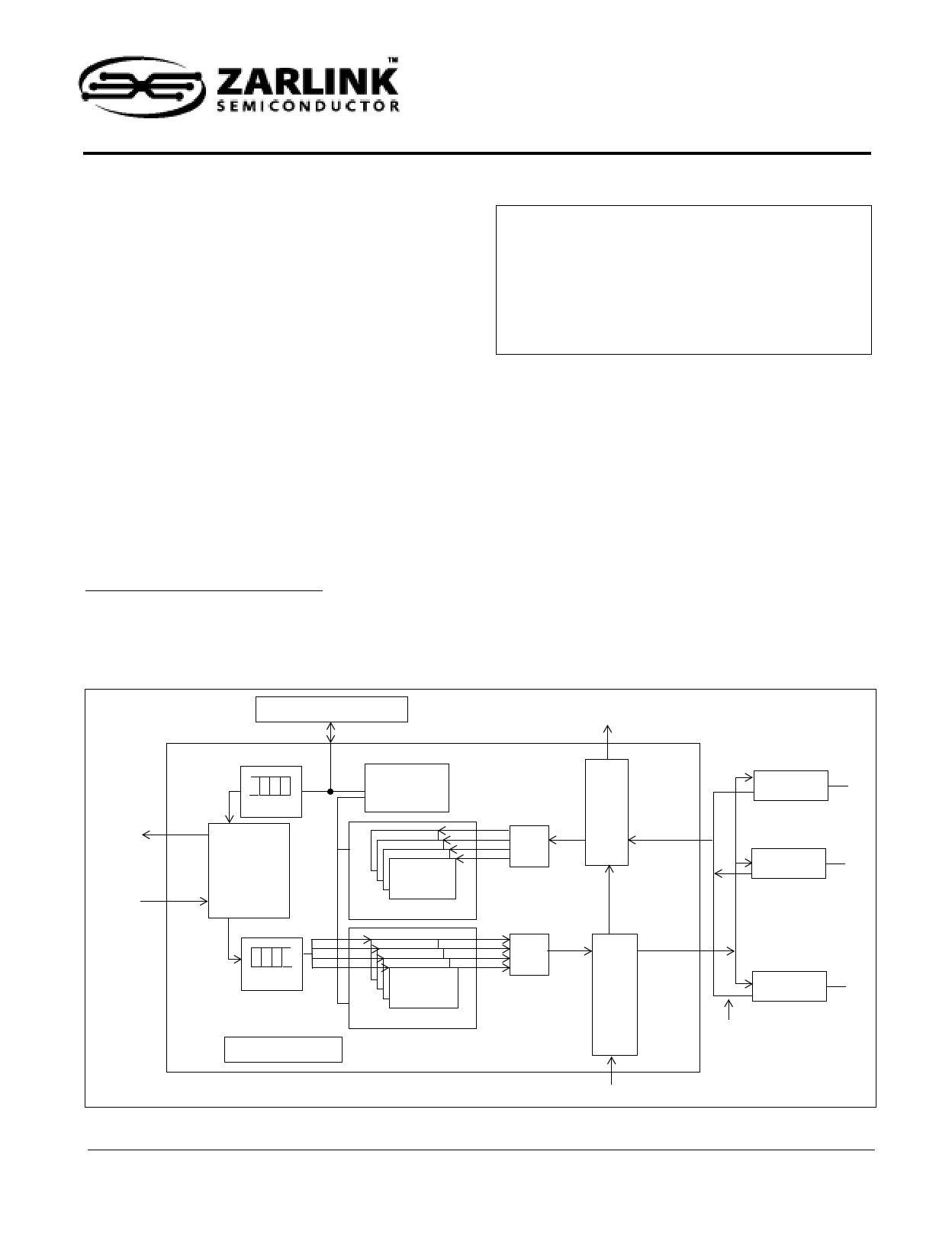
RX External Static RAM
TDM Ring
RX
Utopia
Level 2
BUS
TX
Rx Utopia
FIFo
Utopia
I/F CTRL
Internal IMA
Processors
(1 per group)
TDM
Ring
Control
S/P
Cell
Delineator
CD Circuits (1 per link)
xDSL
xDSL
Tx Utopia
FIFo
Processor I/F
Transmission
Convergence
TC Circuits (1 per link)
P/S
TDM
Ring
Control
xDSL
Serial TDM Ports
(1 per link, up to 10Mb/s
per link)
TDM Ring
Figure 1 - ZL30226/7/8 Block Diagram with Built-in IMA functions for up to 8 IMA Groups over 4/8/16 links
1
Zarlink Semiconductor Inc.
Zarlink, ZL and the Zarlink Semiconductor logo are trademarks of Zarlink Semiconductor Inc.
Copyright 2004, Zarlink Semiconductor Inc. All Rights Reserved.
1 page 
ZL30226/7/8
Data Sheet
Table of Contents
3.3.15 Link Addition. . . . . . . . . . . . . . . . . . . . . . . . . . . . . . . . . . . . . . . . . . . . . . . . . . . . . . . . . . . . . . . . . . 52
3.3.16 Link Deletion . . . . . . . . . . . . . . . . . . . . . . . . . . . . . . . . . . . . . . . . . . . . . . . . . . . . . . . . . . . . . . . . . 52
3.3.17 Disabling an IMA Group . . . . . . . . . . . . . . . . . . . . . . . . . . . . . . . . . . . . . . . . . . . . . . . . . . . . . . . . . 52
3.4 The ATM Receive Path in TC mode . . . . . . . . . . . . . . . . . . . . . . . . . . . . . . . . . . . . . . . . . . . . . . . . . . . . . 53
4.0 Description of the TDM Interface . . . . . . . . . . . . . . . . . . . . . . . . . . . . . . . . . . . . . . . . . . . . . . . . . . . . . . . . . 53
4.1 Non-Framed Mode . . . . . . . . . . . . . . . . . . . . . . . . . . . . . . . . . . . . . . . . . . . . . . . . . . . . . . . . . . . . . . . . . . 53
4.1.1 Non-Framed Mode - 2.5 Mbps . . . . . . . . . . . . . . . . . . . . . . . . . . . . . . . . . . . . . . . . . . . . . . . . . . . . . 54
4.1.2 Non-Framed Mode - 5.0 Mbps . . . . . . . . . . . . . . . . . . . . . . . . . . . . . . . . . . . . . . . . . . . . . . . . . . . . . 54
4.1.3 Non-Framed Mode - 10.0 Mbps . . . . . . . . . . . . . . . . . . . . . . . . . . . . . . . . . . . . . . . . . . . . . . . . . . . . 54
4.2 Clock format . . . . . . . . . . . . . . . . . . . . . . . . . . . . . . . . . . . . . . . . . . . . . . . . . . . . . . . . . . . . . . . . . . . . . . . 55
4.3 TDM Loopback Mode . . . . . . . . . . . . . . . . . . . . . . . . . . . . . . . . . . . . . . . . . . . . . . . . . . . . . . . . . . . . . . . . 55
4.4 .Serial to Parallel (S/P) and Parallel to Serial (P/S) Converters . . . . . . . . . . . . . . . . . . . . . . . . . . . . . . . . 55
4.5 Clocking Options . . . . . . . . . . . . . . . . . . . . . . . . . . . . . . . . . . . . . . . . . . . . . . . . . . . . . . . . . . . . . . . . . . . . 55
4.5.1 Primary and Secondary Reference Signals . . . . . . . . . . . . . . . . . . . . . . . . . . . . . . . . . . . . . . . . . . . 56
4.5.2 Verification of Clock Activity . . . . . . . . . . . . . . . . . . . . . . . . . . . . . . . . . . . . . . . . . . . . . . . . . . . . . . . 56
4.5.3 Clock Selection . . . . . . . . . . . . . . . . . . . . . . . . . . . . . . . . . . . . . . . . . . . . . . . . . . . . . . . . . . . . . . . . 56
5.0 UTOPIA Interface Operation . . . . . . . . . . . . . . . . . . . . . . . . . . . . . . . . . . . . . . . . . . . . . . . . . . . . . . . . . . . . . 57
5.1 ATM Input Port . . . . . . . . . . . . . . . . . . . . . . . . . . . . . . . . . . . . . . . . . . . . . . . . . . . . . . . . . . . . . . . . . . . . . 57
5.2 ATM Output Port . . . . . . . . . . . . . . . . . . . . . . . . . . . . . . . . . . . . . . . . . . . . . . . . . . . . . . . . . . . . . . . . . . . . 58
5.3 UTOPIA Operation With a Single PHY . . . . . . . . . . . . . . . . . . . . . . . . . . . . . . . . . . . . . . . . . . . . . . . . . . . 59
5.4 UTOPIA Operation with Multiple PHY . . . . . . . . . . . . . . . . . . . . . . . . . . . . . . . . . . . . . . . . . . . . . . . . . . . . 59
5.5 UTOPIA Operation in TC Mode. . . . . . . . . . . . . . . . . . . . . . . . . . . . . . . . . . . . . . . . . . . . . . . . . . . . . . . . . 59
5.6 UTOPIA Operation in IMA Mode . . . . . . . . . . . . . . . . . . . . . . . . . . . . . . . . . . . . . . . . . . . . . . . . . . . . . . . . 59
5.7 UTOPIA Loopback. . . . . . . . . . . . . . . . . . . . . . . . . . . . . . . . . . . . . . . . . . . . . . . . . . . . . . . . . . . . . . . . . . . 59
5.8 Examples of UTOPIA Operation Modes . . . . . . . . . . . . . . . . . . . . . . . . . . . . . . . . . . . . . . . . . . . . . . . . . . 60
6.0 Support Blocks . . . . . . . . . . . . . . . . . . . . . . . . . . . . . . . . . . . . . . . . . . . . . . . . . . . . . . . . . . . . . . . . . . . . . . . 61
6.1 Counter Block . . . . . . . . . . . . . . . . . . . . . . . . . . . . . . . . . . . . . . . . . . . . . . . . . . . . . . . . . . . . . . . . . . . . . . 61
6.1.1 UTOPIA Input I/F counters. . . . . . . . . . . . . . . . . . . . . . . . . . . . . . . . . . . . . . . . . . . . . . . . . . . . . . . . 61
6.1.2 Transmit TDM I/F Counters . . . . . . . . . . . . . . . . . . . . . . . . . . . . . . . . . . . . . . . . . . . . . . . . . . . . . . . 61
6.1.3 Receive TDM I/F Counters. . . . . . . . . . . . . . . . . . . . . . . . . . . . . . . . . . . . . . . . . . . . . . . . . . . . . . . . 62
6.1.4 Access to the Counters . . . . . . . . . . . . . . . . . . . . . . . . . . . . . . . . . . . . . . . . . . . . . . . . . . . . . . . . . . 62
6.1.5 Latching counter mode. . . . . . . . . . . . . . . . . . . . . . . . . . . . . . . . . . . . . . . . . . . . . . . . . . . . . . . . . . . 62
6.2 Interrupt Block . . . . . . . . . . . . . . . . . . . . . . . . . . . . . . . . . . . . . . . . . . . . . . . . . . . . . . . . . . . . . . . . . . . . . . 63
6.2.1 IRQ Master Status and IRQ Master Enable Registers. . . . . . . . . . . . . . . . . . . . . . . . . . . . . . . . . . . 64
6.2.2 IRQ Link Status and IRQ Link Enable Registers . . . . . . . . . . . . . . . . . . . . . . . . . . . . . . . . . . . . . . . 64
6.2.2.1 Bit 8 and 7 of IRQ Link 0 Status and IRQ Link 0 Enable Registers. . . . . . . . . . . . . . . . . . . . 65
6.2.3 IRQ Link TC Overflow Status Registers. . . . . . . . . . . . . . . . . . . . . . . . . . . . . . . . . . . . . . . . . . . . . . 65
6.2.4 IRQ IMA Group Overflow Status and Enable Registers. . . . . . . . . . . . . . . . . . . . . . . . . . . . . . . . . . 66
6.2.5 IRQ IMA Overflow Status and RX UTOPIA IMA Group FIFO Overflow Enable Registers . . . . . . . 66
6.3 Microprocessor Interface Block . . . . . . . . . . . . . . . . . . . . . . . . . . . . . . . . . . . . . . . . . . . . . . . . . . . . . . . . . 66
6.3.1 Access to the Various Registers . . . . . . . . . . . . . . . . . . . . . . . . . . . . . . . . . . . . . . . . . . . . . . . . . . . 66
6.3.2 Direct Access . . . . . . . . . . . . . . . . . . . . . . . . . . . . . . . . . . . . . . . . . . . . . . . . . . . . . . . . . . . . . . . . . . 67
6.3.3 Indirect Access. . . . . . . . . . . . . . . . . . . . . . . . . . . . . . . . . . . . . . . . . . . . . . . . . . . . . . . . . . . . . . . . . 67
6.3.4 Clearing of Status Bits . . . . . . . . . . . . . . . . . . . . . . . . . . . . . . . . . . . . . . . . . . . . . . . . . . . . . . . . . . . 67
6.3.4.1 Toggle Bit . . . . . . . . . . . . . . . . . . . . . . . . . . . . . . . . . . . . . . . . . . . . . . . . . . . . . . . . . . . . . . . . 67
6.4 Cell Preprocessor Block . . . . . . . . . . . . . . . . . . . . . . . . . . . . . . . . . . . . . . . . . . . . . . . . . . . . . . . . . . . . . . 67
6.5 TDM Ring Block. . . . . . . . . . . . . . . . . . . . . . . . . . . . . . . . . . . . . . . . . . . . . . . . . . . . . . . . . . . . . . . . . . . . . 68
6.6 SRAM decoding for ZL30226 and ZL30227 . . . . . . . . . . . . . . . . . . . . . . . . . . . . . . . . . . . . . . . . . . . . . . . 69
7.0 Register Descriptions . . . . . . . . . . . . . . . . . . . . . . . . . . . . . . . . . . . . . . . . . . . . . . . . . . . . . . . . . . . . . . . . . . 69
7.1 Register Summary. . . . . . . . . . . . . . . . . . . . . . . . . . . . . . . . . . . . . . . . . . . . . . . . . . . . . . . . . . . . . . . . . . . 69
7.2 Detailed Register Description . . . . . . . . . . . . . . . . . . . . . . . . . . . . . . . . . . . . . . . . . . . . . . . . . . . . . . . . . . 73
7.3 Modes of Operation . . . . . . . . . . . . . . . . . . . . . . . . . . . . . . . . . . . . . . . . . . . . . . . . . . . . . . . . . . . . . . . . . 117
5
Zarlink Semiconductor Inc.
5 Page 
ZL30226/7/8
Pin Diagram - ZL30226
The ZL30226 uses a 384 pin PBGA with a 1.0 mm ball pitch.
Data Sheet
26 25 24 23 22 21 20 19 18 17 16 15 14 13 12 11 10
9
8
7
6
5
4
3
2
1
A
DSTi[4] NC VDD5 NC NC
IC TXRing- TXRing- TXRing- sr_cs_1 sr_a[1] sr_a[4] VDD5 sr_a[7] sr_a sr_a sr_a VDD5 sr_d[6] NC TMS Reset NC
NC
Data[1] Data[5] Sync
[11] [15] [18]
A
B NC VSS IC NC IC NC DSTi[0] TXRing- TXRing- TXRing- sr_cs_0 sr_a[0] sr_a[3] sr_a[5] sr_a[8] sr_a sr_a sr_d[0] sr_d[3] sr_d[7] TDI TRST Test4 NC VSS NC B
Data[0] Data[4] Data[7]
[12] [16]
C
NC NC VSS RXCKi NC
IC RXCKi Latch TXRing- TXRing- VDD5 NC sr_a[2] sr_a[6] sr_a sr_a sr_a sr_d sr_d[4] Test3 TDO VDD5 NC VSS URx URx
C
[4] [0] Clk Data[2] Data[6]
[10] [14] [17]
[1]
Data[0] Data[2]
D IC NC NC VSS V3.3 NC VDD5 Test2 TXRing- V2.5 TXRing- sr_we V3.3 V2.5 sr_a[9] sr_a V3.3 sr_d[2] sr_d[5] TCK V3.3 VSS VSS URx URx URx D
Data[3]
Clk
[13]
Data[1] Data[3] Data[4]
E NC NC NC V3.3
VSS URx VDD5 URx
Data[5]
Data[6]
E
F VDD5 NC IC NC
V3.3 URx URx URx
Data[7] Data[8] Data[9]
F
G RXCKi DSTi[8] NC
[8]
IC
URxD URxD URxD URxD
ata[10] ata[11] ata[12] ata[13]
G
H VDD5 NC NC NC
URxD URxD URx VDD5
ata[14] ata[15] Par
H
J NC IC IC NC
URx URx
SOC Clav
NC VDD5
J
K IC NC NC V3.3
V2.5 URx- URx URxA
CLK Enb ddr[0]
K
L NC RXCKi DSTi NC
[12] [12]
VSS VSS VSS VSS VSS VSS
URxA URxA URxA URxA
ddr[2] ddr[1] ddr[3] ddr[4]
L
M NC IC NC NC
VSS VSS VSS VSS VSS VSS
UTx VDD5 UTx NC
Data[0]
Data[1]
M
N NC VDD5 IC V2.5
VSS VSS VSS VSS VSS VSS
V3.3 UTx UTx UTx
Data[2] Data[3] Data[4]
N
P NC NC NC V3.3
VSS VSS VSS VSS VSS VSS
V2.5 UTx VDD5 UTx
Data[6]
Data[5]
P
R PD PD NC NC
VSS VSS VSS VSS VSS VSS
UTx UTxD UTxD UTxD
Data[9] ata[10] ata[8] ata[7]
R
T PD PD PD NC
VSS VSS VSS VSS VSS VSS
UTxD VDD5 UTxD UTxD
ata[13]
ata[12] ata[11]
T
U PD DSTo TXCKio V2.5
[12] [12]
V3.3 UTxPar UTxD UTxD
ata[15] ata[14]
U
V VDD5 PD NC PD
UTxClk UTx
Enb
UTx UTx
Clav SOC
V
W PD NC PD PD
UTx UTx UTx UTx W
Addr[2] Addr[3] Addr[1] Addr[0]
Y NC PD PD DSTo
[8]
UTx REFCK VDD5 NC
Addr[4] [0]
Y
AA TXCKio VDD5 PD
[8]
V3.3
REFCK REFCK NC REFCK AA
[2] [3]
[1]
AB NC PD PD VSS
V3.3 VDD5 PLL PLL AB
REF[1] REF[0]
AC NC PD NC VSS V3.3 PD NC VDD5 NC V3.3 RXRing RXRing V2.5 V3.3 up_a up_a[7] V2.5 up_irq NC up_d V3.3 VSS VSS NC NC Clk AC
Data[7] Data[4]
[10]
[10]
AD PD VDD5 VSS NC NC NC PD PD PD DSTo PD VDD5 RXRing up_oe VDD5 up_a[6] up_a[3] up_a[0] up_d up_d up_d[8] up_d[5] up_d[2] VSS NC Test1 AD
[0] Data[1] or up_rd
[14] [11]
AE NC VSS NC NC PD DSTo NC NC PD NC RXRing RXRing RXRing up_cs up_a up_a[8] up_a[4] up_a[1] up_d up_d VDD5 up_d[6] up_d[4] up_d[1] VSS NC AE
[4]
Data[6] Data[3] Data[0]
[11]
[15] [12]
AF NC NC NC NC TXCKio PD PD PD TXCKio RXRing RXRing RXRing RXRing up_r/w up_a[9] up_a[5] up_a[2] VDD5 up_d up_d[9] up_d[7] NC up_d[3] up_d[0]
[4]
[0] Data[5] Data[2] Sync Clk
or
[13]
up_wr
26 25 24 23 22 21 20 19 18 17 16 15 14 13 12 11 10
9
8
7
6
5
4
3
2
1
AF
Figure 2 - ZL30226 Pinout (Bottom View)
11
Zarlink Semiconductor Inc.
11 Page | ||
| Páginas | Total 30 Páginas | |
| PDF Descargar | [ Datasheet ZL30227.PDF ] | |
Hoja de datos destacado
| Número de pieza | Descripción | Fabricantes |
| ZL30226 | (ZL30226 - ZL30228) 4/8/16 Port IMA/TC PHY Device | Zarlink Semiconductor |
| ZL30227 | (ZL30226 - ZL30228) 4/8/16 Port IMA/TC PHY Device | Zarlink Semiconductor |
| ZL30228 | (ZL30226 - ZL30228) 4/8/16 Port IMA/TC PHY Device | Zarlink Semiconductor |
| Número de pieza | Descripción | Fabricantes |
| SLA6805M | High Voltage 3 phase Motor Driver IC. |
Sanken |
| SDC1742 | 12- and 14-Bit Hybrid Synchro / Resolver-to-Digital Converters. |
Analog Devices |
|
DataSheet.es es una pagina web que funciona como un repositorio de manuales o hoja de datos de muchos de los productos más populares, |
| DataSheet.es | 2020 | Privacy Policy | Contacto | Buscar |