|
|
|
PDF TD350 Data sheet ( Hoja de datos )
| Número de pieza | TD350 | |
| Descripción | Advanced IGBT/MOSFET Driver | |
| Fabricantes | ST Microelectronics | |
| Logotipo | ||
Hay una vista previa y un enlace de descarga de TD350 (archivo pdf) en la parte inferior de esta página. Total 11 Páginas | ||
|
No Preview Available !
www.DataSheet4U.com
TD350
Advanced IGBT/MOSFET Driver
s 0.75A source/1.2A sink min gate drive
s Active Miller clamp feature
s Two steps turn-off with adjustable level
and delay
s Desaturation detection
s Fault status output
s Negative gate drive ability
s Input compatible with pulse transformer or
optocoupler
s Separate sink and source outputs for easy
gate drive
s UVLO protection
s 2kV ESD protection
Description
TD350 is an advanced gate driver for IGBT and
power MOSFET. Control and protection functions
are included and allow the design of high reliability
systems.
Innovative active Miller clamp function avoids the
need of negative gate drive in most applications
and allows the use of a simple bootstrap supply
for the high side driver
TD350 includes a two-level turn-off feature with
adjustable level and delay. This function protects
against excessive overvoltage at turn-off in case
of overcurrent or short-circuit condition. Same
delay is applied at turn-on to prevent pulse width
distortion.
TD350 also includes an IGBT desaturation
protection and a FAULT status output.
TD350 is compatible with both pulse transformer
and optocoupler signals.
Order Codes
Part Number
TD350ID
TD350IDT
Temperature Range
-40, +125°C
Applications
s 1200V 3-Phase Inverter
s Motor Control
s UPS Systems
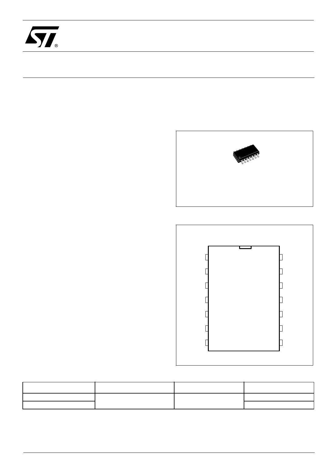
D
SO-14
(Plastic MicroPackage)
Pin Connections (top view)
IN
VREF
FAULT
NC
COFF
NC
LVOFF
1
2
3
4
5
6
7
TD350
14 DESAT
13 VH
12 OUTH
11 OUTL
10 VL
9 CLAMP
8 GND
Package
SO
Packaging
Tube
Tape & Reel
August 2004
Revision 1
1/11
1 page 
Functional Description
TD350
4 Functional Description
4.1 Input
The input is compatible with optocouplers or pulse
transformers. The input is triggered by the signal
edge and allows the use of low-sized, low-cost
pulse transformer. Input is active low (output is
high when input is low) to ease the use of
optocoupler. When driven by a pulse transformer,
the input pulse (positive and negative) width must
be larger than the minimum pule width tonmin.
4.2 Voltage reference
A voltage reference is used to create accurate
timing for the two-level turn-off with external
resistor and capacitor.
4.3 Desaturation protection
Desaturation protection ensures the protection of
the IGBT in the event of overcurrent. When the
DESAT voltage goes higher that 7V, the output is
driven low (with 2-level turn-off if applicable). The
FAULT output is activated. The FAULT state is
exited at the next falling edge of IN input.
A programmable blanking time is used to allow
enough time for IGBT saturation. Blanking time is
provided by an internal current source and
external capacitor.
DESAT input can also be used with an external
comparator for overcurrent or over temperature
detection.
4.4 Active Miller clamp
A Miller clamp allows the control of the Miller
current during a high dV/dt situation and can avoid
the use of a negative supply voltage.
During turn-off, the gate voltage is monitored and
the clamp output is activated when gate voltage
goes below 2V (relative to GND). The clamp
voltage is VL+3V max for a Miller current up to
500mA. The clamp is disabled when the IN input
is triggered again.
4.5 Two level turn-off
The two-level turn-off is used to increase the
reliability of the application.
During turn-off, gate voltage can be reduced to a
programmable level in order to reduce the IGBT
current (in the event of over-current). This action
avoids both dangerous overvoltage across the
IGBT, and RBSOA problems, especially at short
circuit turn-off.
Turn-off (Ta) delay is programmable through an
external resistor and capacitor for accurate timing.
Turn-off delay (Ta) is also used to delay the input
signal to prevent distortion of input pulse width.
4.6 Minimum ON time
In order to ensure the proper operation of the 2-
level turn-off function, the input ON time (Twin)
must be greater than the Twinmin value:
Twinmin=Ta+2*Rdel*Coff
Rdel is the internal discharge resistor and Coff is
the external timing capacitor.
Input signals smaller than Ta are ignored. Input
signals larger than Twinmin are transmitted to the
output stage after the Ta delay with minimum
width distortion (∆Tw=Twout-Twin).
For an input signal width Twin between Ta and
Twinmin, the output width Twout is reduced below
Twin (pulse distortion) and the IGBT could be
partially turned on. These input signals should be
avoided during normal operation.
4.7 Output
The output stage is able to sink 2.3A and source
1.5A typical at 25°C (1.2A/0.75A minimum over
the full temperature range). Separated sink and
source outputs allow independent gate charge
and discharge control without an extra external
diode.
5/11
5 Page 
Revision History
9 Revision History
Date
01 August 2004
Revision
1
First Release
Description of Changes
TD350
Information furnished is believed to be accurate and reliable. However, STMicroelectronics assumes no responsibility for the consequences
of use of such information nor for any infringement of patents or other rights of third parties which may result from its use. No license is granted
by implication or otherwise under any patent or patent rights of STMicroelectronics. Specifications mentioned in this publication are subject
to change without notice. This publication supersedes and replaces all information previously supplied. STMicroelectronics products are not
authorized for use as critical components in life support devices or systems without express written approval of STMicroelectronics.
The ST logo is a registered trademark of STMicroelectronics
All other names are the property of their respective owners
© 2004 STMicroelectronics - All rights reserved
STMicroelectronics group of companies
Australia - Belgium - Brazil - Canada - China - Czech Repubic - Finland - France - Germany - Hong Kong - India - Israel - Italy - Japan -
Malaysia - Malta - Morocco - Singapore - Spain - Sweden - Switzerland - United Kingdom - United States of America
www.st.com
11/11
11 Page | ||
| Páginas | Total 11 Páginas | |
| PDF Descargar | [ Datasheet TD350.PDF ] | |
Hoja de datos destacado
| Número de pieza | Descripción | Fabricantes |
| TD350 | Advanced IGBT/MOSFET Driver | ST Microelectronics |
| TD350E | Advanced IGBT/MOSFET driver | STMicroelectronics |
| TD351 | Advanced IGBT/MOSFET Driver | ST Microelectronics |
| TD352 | Advanced IGBT/MOSFET Driver | ST Microelectronics |
| Número de pieza | Descripción | Fabricantes |
| SLA6805M | High Voltage 3 phase Motor Driver IC. |
Sanken |
| SDC1742 | 12- and 14-Bit Hybrid Synchro / Resolver-to-Digital Converters. |
Analog Devices |
|
DataSheet.es es una pagina web que funciona como un repositorio de manuales o hoja de datos de muchos de los productos más populares, |
| DataSheet.es | 2020 | Privacy Policy | Contacto | Buscar |