|
|
|
PDF MAS9191EB Data sheet ( Hoja de datos )
| Número de pieza | MAS9191EB | |
| Descripción | EVALUATION BOARD | |
| Fabricantes | MAS | |
| Logotipo | ||
Hay una vista previa y un enlace de descarga de MAS9191EB (archivo pdf) en la parte inferior de esta página. Total 16 Páginas | ||
|
No Preview Available !
www.DataSheet4U.com
DA9191EB.006
June 30,1997
MAS9191EB
EVALUATION BOARD FOR CELLULAR BASEBAND ICs
• Audio/Data Processor and all necessary external components
• Battery Management IC and battery protection/charging circuit
• VCTCXO with DAC voltage control
• uP with evaluation software
DESCRIPTION
The Cellular Baseband evaluation board includes
MAS9191A (Audio/Data Processor), MAS9129
(Battery Management) and MS8323 (VCTCXO) ICs
with all needed external components and software.
The two regulators of MAS9129 provide all the power
for the board. The board has BNC connectors for
typical MAS9191A interfaces. By using customised
software and external RF parts the complete
evaluation of an AMPS/ ETACS/ NAMPS phone can
be performed. A general purpose micro controller is
used to control the MAS9191A internal registers
through a serial bus interface. For the micro controller
there is 32kB SRAM, 64kB FLASH, an LCD, a keypad
and an RS-232-C interface for software downloading
to SRAM or FLASH. There is also a direct interface to
the MAS9191A serial bus allowing an external
controller to be used.
FEATURES
• Fully operational system (only NiCd/NiMH battery
or power supply needed)
• Connectors to Rx,Tx,microphone, ear piece, etc.
• Several test points for audio block
• Battery charger input (9.0VDC/265mA)
• Micro controller with 32kB SRAM, 64kB FLASH
• Keyboard and 2-line/16-character LCD
• RS-232-C interface for software downloading
• External micro controller connector
• 3.4 - 9.0 NiCd/NiMH battery input or power supply
MEASUREMENTS
• Regulator voltage and current
• Receive and transmit frequency responses
• Send and receive messages
• Microphone and Rx audio levels
• SAT detection and generation
• Signalling Tone level
• DTMF detection and generation
• Gain control levels
• Expander and compressor functionality
• VCTCXO output signal
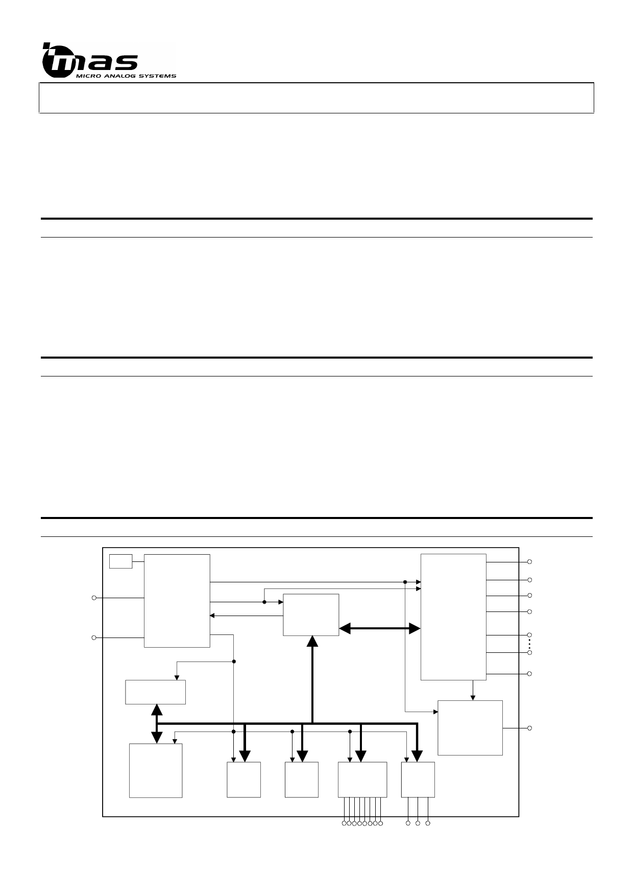
BLOCK DIAGRAM
ON/OFF
SWITCH
BATTERY
INPUT
(3.4 -9.0 VDC)
MAS9129
3.0V/50mA
LDO2
BATTERY
MANAGEMENT
XRESET
WATCHDOG
BATTERY
CHARGER
(9.0 VDC/265mA)
3.0V/100mA
LDO1
MICRO
CONTROLLER
SERIAL
INTERFACE
MAS9191A MIC
BUZZER
AUDIO/DATA
PROCESSOR
EAR PIECE
TEST
POINTS
RX
LCD DISPLAY
DAC
Vcont
MS8323
VCTCXO
TX
OSC
OUT
KEYPAD
SRAM
32kB
FLASH
64kB
I/O
PORT
RS232C
RxD DTR TxD
1
1 page 
CONNECTOR DESCRIPTION
DA9191EB.006
June 30,1997
Connector name
Battery
S1
CM1
CM2
MIC
J1
J2
EXTMIC
T2
T3
T4
T5
CM3
CM4
CM5
Pin Function
NiCd Battery or external DC power supply capable of driving at least 200 mA current is
connected to battery input.
B+ Positive supply voltage from 3.4 V to 9.0V DC.
B- Ground.
ON/OFF power switch for MAS9129 voltage regulators.
This jumper is normally closed, but can be opened to use an external current meter to
measure the power consumption of the digital section.
1 Regulator 1 output.
2 VDD input.
This jumper is normally closed, but can be opened to use an external current meter to
measure the power consumption of the analog section.
1 Regulator 2 output.
2 VDD input.
The microphone is normally connected to this connector. See the microphone function.
1 Microphone input.
2 Ground.
The internal/external microphone select switches.
1 Microphone amplifier feedback signal. Connect to pin 3 to use the mounted
microphone. Otherwise, connect the external microphone circuit feedback
signal to this pin.
2 Microphone amplifier input. Connect this to pin 4 to use the mounted
microphone. Otherwise, connect the external microphone output signal to this
pin.
3 Feedback signal input for the assembled microphone circuit.
4 Microphone output signal for the assembled microphone circuit.
Use jumper to enable regulator 2.
BNC-type connector for external microphone source.
1 External microphone input.
2 Ground.
MICOUT signal is the output from the section which contains the following blocks: Filter F8,
Gain Control GC3 and Filter F9. The source for the signal is either from SGND, Microphone
amplifier A6, EXTMIC input or from DTMF generator.
COUT is the compressor output signal. The compressor and all the blocks before T2 can be
measured by using this test point.
LPFIN test point can be used as an output to measure gain controls GC4 and GC5, the filter
F10 and all the blocks before T3.
TAUDOUT is the output from the TX audio block.
1 VDD from regulator 2.
2 MASVDD. Power input for MAS9191A. Current measurement point.
1 Battery and charging voltage output.
2 Power input for MAS9129. Current measurement point.
1 VDD from regulator 2.
2 Power input for MS8323. Current measurement point.
5
5 Page 
SCHEMATIC DIAGRAMS
DA9191EB.006
June 30,1997
11
11 Page | ||
| Páginas | Total 16 Páginas | |
| PDF Descargar | [ Datasheet MAS9191EB.PDF ] | |
Hoja de datos destacado
| Número de pieza | Descripción | Fabricantes |
| MAS9191EB | EVALUATION BOARD | MAS |
| Número de pieza | Descripción | Fabricantes |
| SLA6805M | High Voltage 3 phase Motor Driver IC. |
Sanken |
| SDC1742 | 12- and 14-Bit Hybrid Synchro / Resolver-to-Digital Converters. |
Analog Devices |
|
DataSheet.es es una pagina web que funciona como un repositorio de manuales o hoja de datos de muchos de los productos más populares, |
| DataSheet.es | 2020 | Privacy Policy | Contacto | Buscar |