|
|
|
PDF RE46C109 Data sheet ( Hoja de datos )
| Número de pieza | RE46C109 | |
| Descripción | Voltage Converter and Piezoelectric Horn Driver | |
| Fabricantes | R & E International | |
| Logotipo | ||
Hay una vista previa y un enlace de descarga de RE46C109 (archivo pdf) en la parte inferior de esta página. Total 8 Páginas | ||
|
No Preview Available !
www.DataSheet4U.com
R&E International
RE46C109
Voltage Regulator, Voltage Converter and Piezoelectric Horn Driver
Product Specification
General Description
The RE46C109 is intended for use in applications
where low voltage regulation and a high voltage
horn driver are required. The circuit features a
voltage boost converter/regulator and driver circuit
suitable for driving a piezoelectric horn. The horn
enable pin activates the boost converter and horn
driver circuit. Supply current is 6.5uA maximum
when the boost regulator and horn driver are not in
use. A 3V regulator is also provided for
microprocessor voltage regulation. Low battery
detection and signaling are also available.
Interconnect pins are provided to allow
communication in multiple unit environments. A
power good pin monitors the status of the regulator
output.
Applications
Smoke detectors
CO Detectors
Personal Security Products
Electronic Games
Hand Held Instruments
Features
• Low Quiescent Current
• 12V Boost Regulator
• Low Horn Driver Ron
• 3V Regulator, Other Options Available
• Low Battery Detection Interface
• Power Good and Brownout Circuits
• Device interconnection
• Available in DIP and SOIC packages
• Available in Standard Packaging or RoHS
Compliant Pb Free Packaging
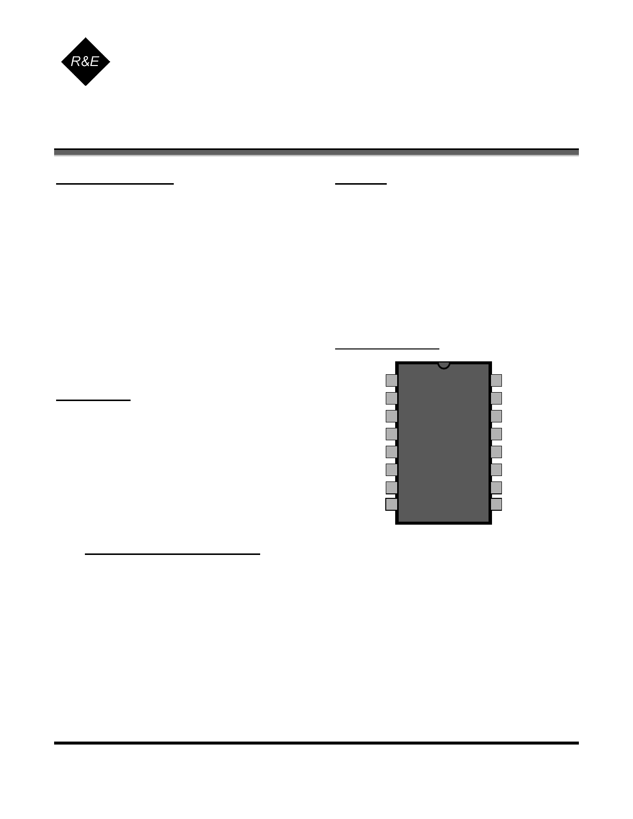
Pin Configuration
VDD
IO1
IODIR
IO2
LBST
PG
HRNEN
VSS
1
16 VPOS
CAP+
CAP-
VREG
LBAT
HORNB
HORNS
FEED
ABSOLUTE MAXIMUM RATINGS
PARAMETER
Supply Voltage
Input Voltage Range Except FEED, IO1, IO2
FEED Input Voltage Range
IO2 Input Voltage Range
IO1 (as input) Voltage Range
Input Current except FEED
Operating Temperature
Continuous Operating Current (Horn or VPOS)
Storage Temperature
Maximum Junction Temperature
SYMBOL
VDD
Vin
Vinfd
Vio2
Vio1
Iin
TA
Icon
TSTG
TJ
VALUE
12
-.3 to Vdd +.3
-10 to +22
-.3 to VREG+.3
-.3 to Vdd + 6
10
-40 to 85
50
-55 to 125
125
UNITS
V
V
V
V
V
mA
°C
mA
°C
°C
Stresses beyond those listed under Absolute Maximum Ratings may cause permanent damage to the device. These are
stress ratings only and operation at these conditions for extended periods may affect device reliability.
This product utilizes CMOS technology with static protection; however proper ESD prevention procedures should be used
when handling this product. Damage can occur when exposed to extremely high static electrical charges.
Telephone 610.992.0727
Facsimile 610.992.0734
E-mail: [email protected]
Page 1 of 8
DS-RE46C109-011207
This datasheet contains PROPRIETARY and CONFIDENTIAL information.
1 page 
RE46C109
Voltage Regulator, Voltage Converter and Piezoelectric Horn Driver
Product Specification
R&E International
PIN DESCRIPTIONS
VDD (Pin 1, Input) - Connect to the positive
terminal of the supply voltage for the voltage
regulator, charge pump voltage converter
and bi-directional Interconnect block.
IO1 (Pin 2, Input/Output) - This bi-directional
pin provides an interface to additional
RE46C109 IO1 pins. This serves as a
communication link between separate
modules.
IODIR (Pin 3, Input) - This input provides
control for the bi-directional pins IO1 and
IO2.
IO2 (Pin 4, Input/Output) - This bi-directional
pin provides an interface to a TTL/CMOS I/O
of a uP or ASIC. Refer to the interconnect
logic truth table.
LBST (Pin 5, Input) - This input provides an
enable or strobe control for the analog low
battery detection function.
PG (Pin 6, Output) - This open drain NMOS
output provides a status indication of when
the VREG output is above or below a
specified voltage level.
HRNEN (Pin 7, Input) - This input provides
activation control for the charge pump boost
regulator and horn driver outputs.
VSS (Pin 8, Input) - This power pin is
connected to the negative terminal of the
supply voltage.
FEEDBACK (Pin9, Input) - Horn driver
input.
HORNS (Pin10, Output) - Horn output driver
which provides VPOS to VSS output voltage
swing for the piezoelectric horn.
HORNB (Pin11, Output) - Horn output driver
which provides VPOS to VSS output voltage
swing for the piezoelectric horn.
LBAT (Pin12, Output) - Analog output
voltage that is proportional to the VDD
supply and functions as a low battery
detection output.
VREG (Pin13, Output) - Voltage regulator
output, requires an external capacitor.
VCAP- (Pin14, I/O) - Negative terminal for
the external charge pump boost (fly)
capacitor.
VCAP+ (Pin 15, I/O) - Positive terminal for
the external charge pump boost (fly)
capacitor.
VPOS (Pin 16, Output) - This output pin
requires an external filter capacitor which
supplies voltage for the horn driver outputs.
Telephone 610.992.0727
Facsimile 610.992.0734
E-mail: [email protected]
Page 5 of 8
DS-RE46C109-011207
This datasheet contains PROPRIETARY and CONFIDENTIAL information.
5 Page | ||
| Páginas | Total 8 Páginas | |
| PDF Descargar | [ Datasheet RE46C109.PDF ] | |
Hoja de datos destacado
| Número de pieza | Descripción | Fabricantes |
| RE46C100 | Piezoelectric Horn Driver Circuit | R & E International |
| RE46C100 | Piezoelectric Horn Driver Circuit | Microchip |
| RE46C101 | Piezoelectric Horn Driver and LED Driver Circuit | ETC |
| RE46C102 | CMOS Dual H-Bridge Driver | R & E International |
| Número de pieza | Descripción | Fabricantes |
| SLA6805M | High Voltage 3 phase Motor Driver IC. |
Sanken |
| SDC1742 | 12- and 14-Bit Hybrid Synchro / Resolver-to-Digital Converters. |
Analog Devices |
|
DataSheet.es es una pagina web que funciona como un repositorio de manuales o hoja de datos de muchos de los productos más populares, |
| DataSheet.es | 2020 | Privacy Policy | Contacto | Buscar |