|
|
|
PDF VND5050K-E Data sheet ( Hoja de datos )
| Número de pieza | VND5050K-E | |
| Descripción | Double channel high side driver | |
| Fabricantes | ST Microelectronics | |
| Logotipo | ||
Hay una vista previa y un enlace de descarga de VND5050K-E (archivo pdf) en la parte inferior de esta página. Total 28 Páginas | ||
|
No Preview Available !
www.DataSheet4U.com
VND5050J-E
VND5050K-E
Double channel high side driver with analog current sense
for automotive applications
Features
General
Max supply voltage
Operating voltage range
Max On-State resistance (per ch.)
Current limitation (typ)
Off state supply current
VCC
VCC
RON
ILIMH
IS
41V
4.5 to 36V
50 mΩ
19 A
2 µA(*)
(*) Typical value with all loads connected
Application
■ All types of resistive, inductive and capacitive
loads
Main
■ Inrush current active management by power
limitation
■ Very low stand-by current
■ 3.0V CMOS compatible input
■ Optimized electromagnetic emission
■ Very low electromagnetic susceptibility
■ In compliance with the 2002/95/ec european
directive
Diagnostic Functions
■ Open drain status output
■ On state open load detection
■ Off state open load detection
■ Thermal shutdown indication
Protections
■ Undervoltage shut-down
■ Overvoltage clamp
■ Output stuck to VCC detection
■ Load current limitation
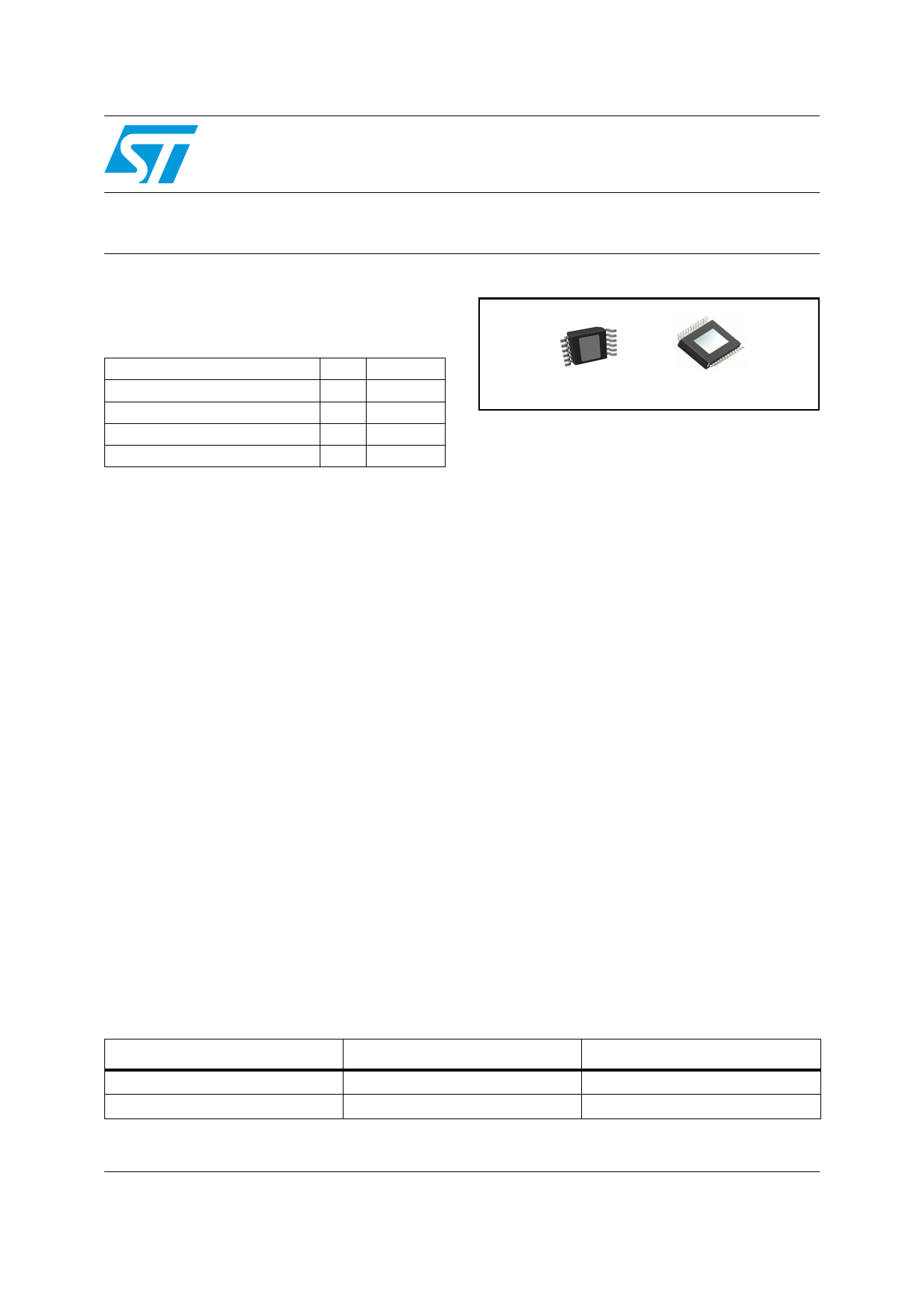
PowerSSO-12 PowerSSO-24
■ Self limiting of fast thermal transients
■ Protection against loss of ground and loss of
VCC
■ Thermal shut down
■ Reverse battery protection (see Figure 28)
■ Electrostatic discharge protection
Description
The VND5050K-E and VND5050J-E is a
monolithic device made using STMicroelectronics
VIPower M0-5 technology. It is intended for driving
resistive or inductive loads with one side
connected to ground. Active VCC pin voltage
clamp protects the device against low energy
spikes (see ISO7637 transient compatibility
table). The device detects open load condition
both in on and off state, when STAT_DIS is left
open or driven low. Output shorted to VCC is
detected in the off state.
When STAT_DIS is driven high, STATUS pin is in
high impedance state.
Output current limitation protects the device in
overload condition. In case of long overload
duration, the device limits the dissipated power to
safe level up to thermal shut-down intervention.
Thermal shut-down with automatic restart allows
the device to recover normal operation as soon as
fault condition disappears..
Order codes
Package
PowerSSO-12
PowerSSO-24
Part number (Tube)
VND5050J-E
VND5050K-E
Part number (Tape & Reel)
VND5050J-E13TR
VND5050K-E13TR
March 2006
Rev 1
1/28
www.st.com
28
1 page 
VND5050J-E / VND5050K-E
2.2 Thermal Data
Table 3. Thermal Data
Symbol
Parameter
Rthj-case
Rthj-amb
Thermal resistance junction-case (Max.)
(with one channel ON)
Thermal resistance junction-ambient (Max.)
Electrical specifications
Value
PowerSSO-12
PowerSSO-24
2.8 2.8
See Figure 31
See Figure 35
Unit
°C/W
°C/W
2.3 Electrical Characteristics
8V<VCC<36V; -40°C<Tj<150°C, unless otherwise specified.
Table 4. Power section
Symbol
Parameter
Test Conditions
Min. Typ. Max. Unit
VCC
VUSD
VUSDhyst
Operating supply voltage
Undervoltage shutdown
Undervoltage shut-down
hysteresis
4.5 13 36
3.5 4.5
0.5
V
V
V
RON
On state resistance(2)
IOUT=2A; Tj=25°C
IOUT=2A; Tj=150°C
IOUT=2A; VCC=5V; Tj=25°C
50 mΩ
100 mΩ
65 mΩ
Vclamp Clamp Voltage
IS=20mA
41 46 52 V
IS Supply current
Off State; VCC=13V; Tj=25°C;
VIN=VOUT=VSENSE=VCSD=0V
On State; VCC=13V; VIN=5V; IOUT=0A
2(1) 5(1) µA
3 6 mA
IL(off1)
IL(off2)
VF
Off state output current(2)
Off state output current(2)
Output - VCC diode voltage(2)
VIN=VOUT=0V; VCC=13V; Tj=25°C
VIN=VOUT=0V; VCC=13V; Tj=125°C
VIN=0V; VOUT=4V
-IOUT=4A; Tj=150°C
0 0.01 3
05
-75 0
0.7
µA
V
(1) PowerMOS leakage included.
(2) For each channel
Table 5. Switching (VCC=13V)
Symbol
Parameter
td(on)
Turn-on delay time
td(off)
Turn-off delay time
dVOUT/dt(on) Turn-on voltage slope
dVOUT/dt(off) Turn-off voltage slope
Test Conditions
RL=6.5Ω (see Figure 5)
RL=6.5Ω (see Figure 5)
RL=6.5Ω
RL=6.5Ω
Min. Typ. Max. Unit
20
40
see Figure 22
see Figure 24
µs
µs
V/µs
V/µs
5/28
5 Page 
VND5050J-E / VND5050K-E
Figure 7. Waveforms
Electrical specifications
INPUT
STAT_DIS
LOAD CURRENT
STATUS
VCC
INPUT
STAT_DIS
LOAD CURRENT
STATUS
VUSD
NORMAL OPERATION
UNDERVOLTAGE
VUSDhyst
undefined
INPUT
STAT_DIS
LOAD VOLTAGE
STATUS
INPUT
STAT_DIS
LOAD VOLTAGE
LOAD CURRENT
STATUS
OPEN LOAD with external pull-up
VOL
VOUT>VOL
OPEN LOAD without external pull-up
IOUT<IOL
tPOL
RESISTIVE SHORT TO Vcc, NORMAL LOAD
INPUT
STAT_DIS
LOAD VOLTAGE
STATUS
Tj
INPUT
STAT_DIS
TR TTSD
TRS
LOAD CURRENT
IOUT>IOL
VOUT>VOL
tDSTKON
OVERLOAD OPERATION
VOL
STATUS
ILIMH
ILIML
current power
limitation limitation
thermal cycling
SHORTED LOAD
NORMAL LOAD
11/28
11 Page | ||
| Páginas | Total 28 Páginas | |
| PDF Descargar | [ Datasheet VND5050K-E.PDF ] | |
Hoja de datos destacado
| Número de pieza | Descripción | Fabricantes |
| VND5050K-E | Double channel high side driver | ST Microelectronics |
| Número de pieza | Descripción | Fabricantes |
| SLA6805M | High Voltage 3 phase Motor Driver IC. |
Sanken |
| SDC1742 | 12- and 14-Bit Hybrid Synchro / Resolver-to-Digital Converters. |
Analog Devices |
|
DataSheet.es es una pagina web que funciona como un repositorio de manuales o hoja de datos de muchos de los productos más populares, |
| DataSheet.es | 2020 | Privacy Policy | Contacto | Buscar |