|
|
PDF VSC834 Data sheet ( Hoja de datos )
| Número de pieza | VSC834 | |
| Descripción | 2.5Gb/s 17 x 17 Crosspoint Switch | |
| Fabricantes | Vitesse Semiconductor | |
| Logotipo | ||
Hay una vista previa y un enlace de descarga de VSC834 (archivo pdf) en la parte inferior de esta página. Total 16 Páginas | ||
|
No Preview Available !
www.DataSheet4U.com
VITESSE
SEMICONDUCTOR CORPORATION
Datasheet
VSC834
2.5Gb/s 17x17 Crosspoint Switch
with Input Signal Activity (ISA) Monitoring
Features
• 17 Input by 17 Output Crosspoint Switch
• 2.5Gb/s NRZ Data Bandwidth
• 42 Gb/s Aggregate Bandwidth
• TTL Compatible µP Interface
• Differential PECL Data Inputs
• On-chip 50Ω Input Terminations
• 50Ω Source Terminated PECL Output Drivers
• Single 3.3V Supply
• 9W Maximum Power Dissipation
• High Performance 256 Pin BGA Package
General Description
The VSC834 is a monolithic 17x17 asynchronous crosspoint switch designed to carry broadband data
streams at up to 2.5Gb/s. The non-blocking switch core is programmed through a parallel microprocessor inter-
face that allows random access programming of each output port. A high degree of signal integrity is main-
tained through the chip through fully differential signal paths.
The crosspoint function is based on a multiplexer tree architecture. Each data output is driven by a 17:1
multiplexer tree that can be programmed to one and only one of its 17 inputs, and each data input can be pro-
grammed to multiple outputs. The signal path is unregistered, so no clock is required for the data inputs. The
signal path is asynchronous, so there are no restrictions on the phase, frequency, or signal pattern at each input.
Each input channel has an activity monitor function that can be used to identify loss of activity (LOA). An inter-
rupt pin is provided to signal LOA, after which an external controller can query the chip to determine the chan-
nel(s) on which the fault occurred.
Each output driver is a fully differential switched current driver with on-die back-terminations for maxi-
mum signal integrity. Data inputs are terminated on die through 50Ω resistors connected to VTERM.
The parallel interface uses TTL levels, and provides address, data, and control pins that are compatible with
a microprocessor-style interface. The control port provides access to all chip functions, including LOA, and
programming. Program buffering is provided to allow multiple program assignments to be queued and issued
simultaneously via a single configure command.
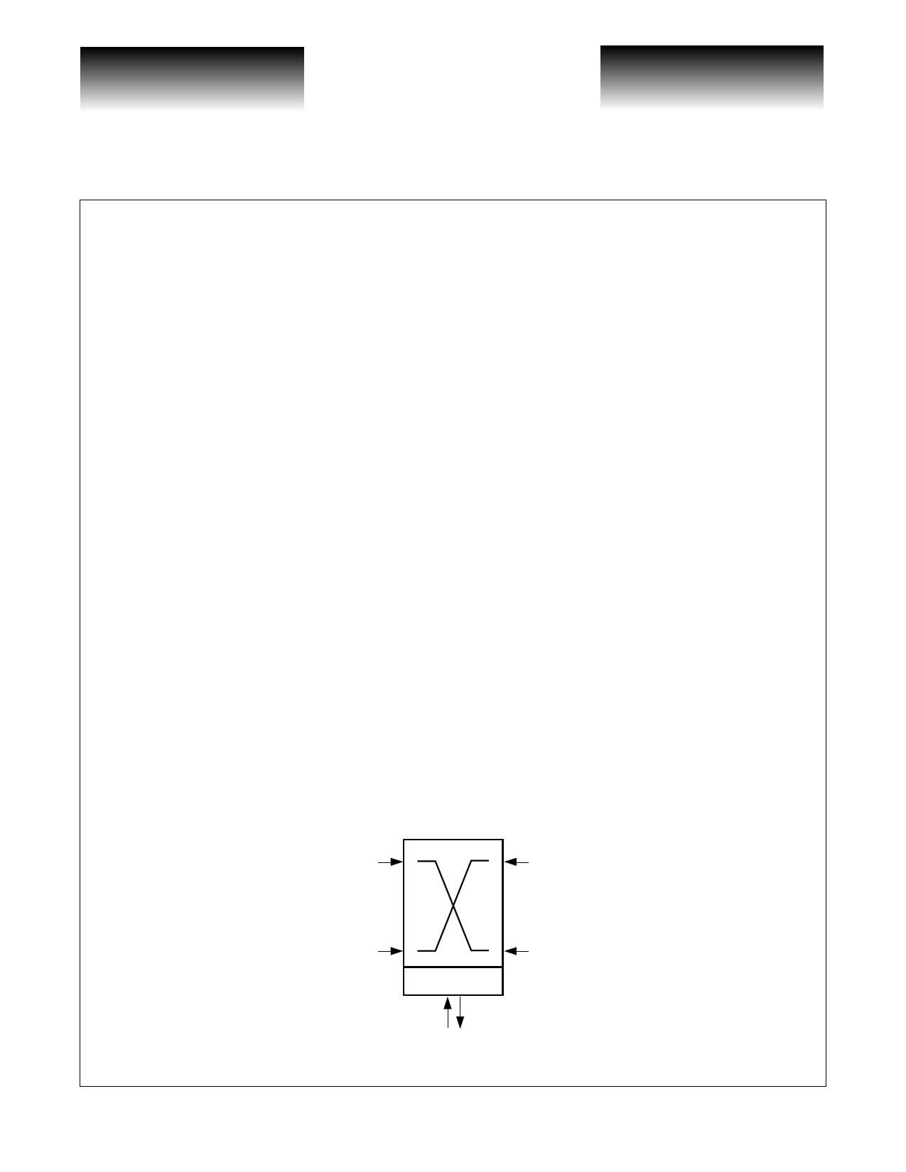
VSC834 Block Diagram
A0 Y0
A16
Control Logic
µP Interface
Y16
G52247-0, Rev 4.2
02/09/01
© VITESSE SEMICONDUCTOR CORPORATION • 741 Calle Plano • Camarillo, CA 93012
Tel: (800) VITESSE • FAX: (805) 987-5896 • Email: [email protected]
Internet: www.vitesse.com
Page 1
1 page 
VITESSE
SEMICONDUCTOR CORPORATION
Datasheet
VSC834
2.5Gb/s 17x17 Crosspoint Switch
with Input Signal Activity (ISA) Monitoring
AC Characteristics
Table 3: Data Path
Parameter
Description
FRATE
TISKW
TOSKW
tR, tF
tR, tF
tjP
Data rate
Input channel delay skew (1)
Output channel delay skew (2)
High-speed input rise/fall times, 20% to 80% (3)
High-speed output rise/fall times, 20% to 80%
Output data eye jitter, peak-peak, 223 PRBS (4)
Min Typ Max Units
- - 2.5 Gb/s
- 300 -
ps
- 300 -
ps
- - 150 ps
- - 150 ps
- - 100 ps
Note: Unless otherwise stated, all specifications are guaranteed but not tested.
Note 1: Skew between any two input channels to a given output.
Note 2: Skew between any two output channels from the same input channel.
Note 3: Required for high-speed output rise/fall spec at FRATE=2.5 Gbits/s. For lower rate signals, use 0.375/FRATE
Note 4: Broadband jitter added to a jitter-free signal; jitter is primarily in the form of ISI for random data
Figure 2: Interrupt Timing (Change in Monitor State Registers)
MONCLK
Monitor State
Monitor State Reg
INTB
CSB
RDB
ADDR[5:0]
DATA[4:0]
TsRDB
ThRDB
TtsDATA
Figure 3: Interrupt Timing (No Change in Monitor State Registers)
MONCLK
Monitor State
Monitor State Reg
INTB
G52247-0, Rev 4.2
02/09/01
© VITESSE SEMICONDUCTOR CORPORATION • 741 Calle Plano • Camarillo, CA 93012
Internet: www.vitesse.com
Page 5
5 Page 
Datasheet
VSC834
VITESSE
SEMICONDUCTOR CORPORATION
2.5Gb/s 17x17 Crosspoint Switch
with Input Signal Activity (ISA) Monitoring
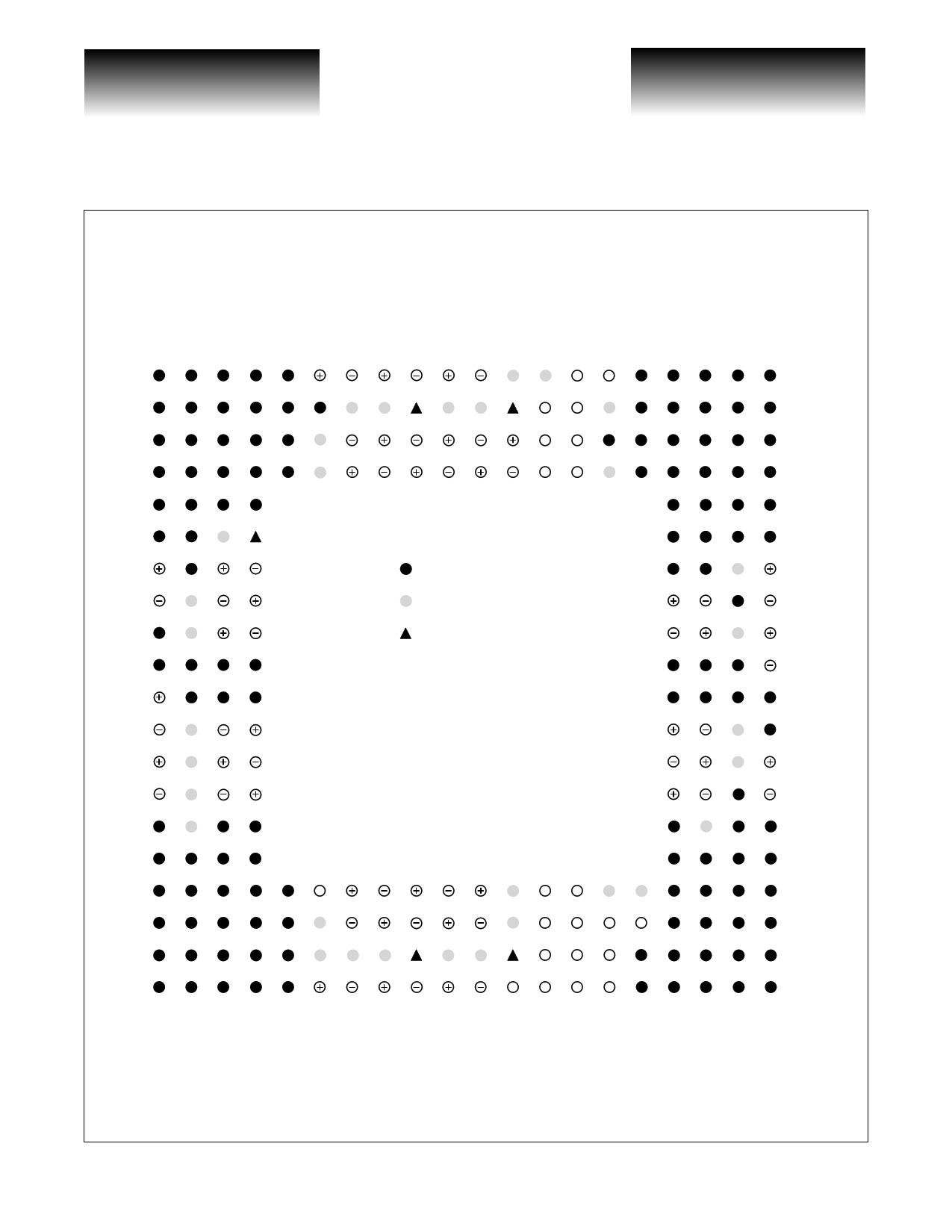
Figure 6: Pinout Diagram
20 19 18 17 16 15 14 13 12 11 10 9 8 7 6 5 4 3
A0 A6 A12
ALE MONCLK
ADR0 ADR3
ADR2 ADR4
A2 A4 A8 A10 A14 A16 ADR1 ADR5
Y0
Y2
Y4
Y6
Y8
Y10
Y12
Y14
Y16
VCC
VEE
VTERM
BOTTOM VIEW
Y3
Y5
Y9
Y11
Y15
VCOML
A3 A5 A9 A11 A15
D2 INTB
D1 D0 VHYS VCOMR
D3 RDB CONFIG
D5 D4 WRB CSB
A1 A7 A13
BALL
2 1 GRID
INDEX
A
B
C
D
E
F
G
Y1
H
J
Y7
K
L
M
N
Y13
P
R
T
U
V
W
Y
G52247-0, Rev 4.2
02/09/01
© VITESSE SEMICONDUCTOR CORPORATION • 741 Calle Plano • Camarillo, CA 93012
Internet: www.vitesse.com
Page 11
11 Page | ||
| Páginas | Total 16 Páginas | |
| PDF Descargar | [ Datasheet VSC834.PDF ] | |
Hoja de datos destacado
| Número de pieza | Descripción | Fabricantes |
| VSC830 | 2.7Gb/s Asynchronous Dual 2x2 Crosspoint Switch | Vitesse Semiconductor |
| VSC834 | 2.5Gb/s 17 x 17 Crosspoint Switch | Vitesse Semiconductor |
| VSC835 | 34x34 Crosspoint Switch | Vitesse Semiconductor |
| VSC837 | 3.2Gb/s 68x68 Crosspoint Switch | Vitesse Semiconductor |
| Número de pieza | Descripción | Fabricantes |
| SLA6805M | High Voltage 3 phase Motor Driver IC. |
Sanken |
| SDC1742 | 12- and 14-Bit Hybrid Synchro / Resolver-to-Digital Converters. |
Analog Devices |
|
DataSheet.es es una pagina web que funciona como un repositorio de manuales o hoja de datos de muchos de los productos más populares, |
| DataSheet.es | 2020 | Privacy Policy | Contacto | Buscar |
