|
|
|
PDF L9942 Data sheet ( Hoja de datos )
| Número de pieza | L9942 | |
| Descripción | Integrated stepper motor driver for bipolar stepper motors | |
| Fabricantes | ST Microelectronics | |
| Logotipo | ||
Hay una vista previa y un enlace de descarga de L9942 (archivo pdf) en la parte inferior de esta página. Total 30 Páginas | ||
|
No Preview Available !
www.DataSheet4U.com
L9942
Integrated stepper motor driver for bipolar stepper motors
with microstepping and programmable current profile
PRELIMINARY DATA
Features
■ Two full bridges for max. 1.3 A load (RDSON =
500 mΩ)
■ Programmable current waveform with look-up
table: 9 entries with 5bit resolution
■ Current regulation by integrated PWM
controller and internal current sensing
■ Programmable stepping mode: Full, Half, Mini
and Microstepping
■ Programmable slew rate for EMC and power
dissipation optimisation
■ Programmable Fast-, Slow-, Mixed-and Auto-
Decay Mode
■ Full-Scale Current programmable with 3bit
resolution
■ Very low current consumption in standby mode
IS < 3µA, typ. Tj ≤ 85 °C
■ All outputs short circuit protected with
Openload, Overloadcurrent, Temperature
Warning and Thermal Shutdown
■ The PWM signal of the internal PWM controller
is available as digital output.
■ All parameters guaranteed for 7V < Vs < 20V
Applications
Stepper Motor Driver for bipolar Stepper Motors in
Automotive Applications like Light Levelling,
Bending Light and Throttle Control.
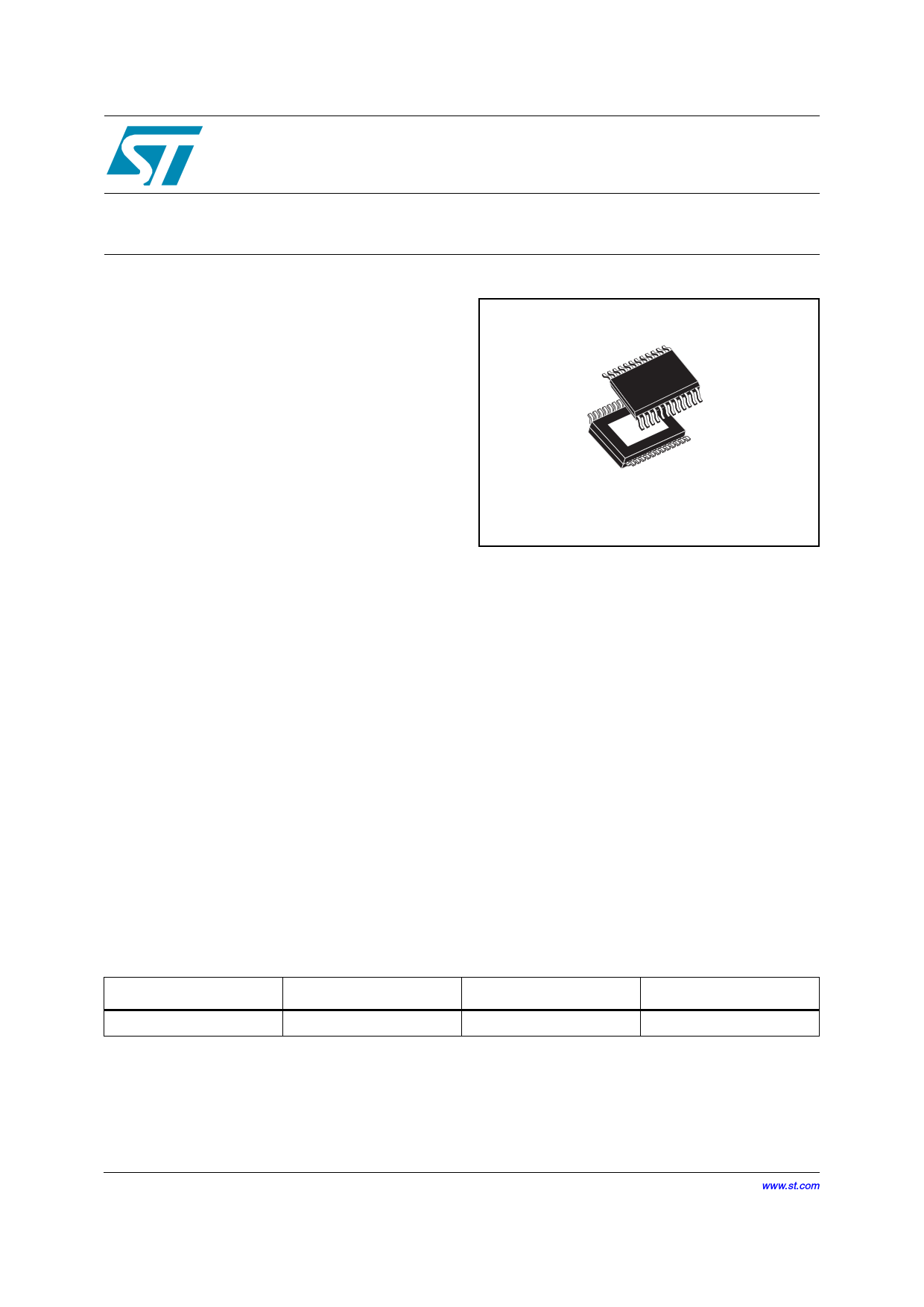
PowerSSO-24
Description
The device is an integrated stepper motor driver
for bipolar stepper motors with microstepping and
programmable current profile look-up-table to
allow a flexible adaptation of the stepper motor
characteristics and intended operating conditions.
It is possible to use different current profiles
depending on target criteria: audible noise,
vibrations, rotation speed or torque. The decay
mode used in PWM-current control circuit can be
programmed to slow-, fast-, mixed-and auto-
decay. In autodecay mode device will use slow
decay mode if the current for the next step will
increase and the fast decay or mixed decay mode
if the current will decrease.
Order codes
Part number
L9942
Junction Temp range, °C
-40 to 150
Package
PowerSSO-24
Packing
Tube
November 2005
This is preliminary information on a new product now in development or undergoing evaluation. Details are subject to
change without notice.
Rev 1
1/37
www.st.com
37
1 page 
L9942
1 Block diagram and Pin information
Table 1. Pin Description
Pin Symbol
Function
1, 12, 13, 24
PGND
Power ground: All pins PGND are internally connected to the heat slug.
Important: All pins of PGND must be externally connected!
3, 10, 15, 22
Power supply voltage (external reverse protection required): For EMI
VS reason a ceramic capacitor as close as possible to PGND is recommended.
Important: All pins of VS must be externally connected !
2, 23
Fullbridge-outputs An: The output is built by a highside and a lowside switch,
which are internally connected. The output stage of both switches is a power
QA1,QA2 DMOS transistor. Each driver has an internal reverse diode (bulk-drain-diode:
highside driver from output to VS, lowside driver from PGND to output). This
output is over-current protected.
11, 14
Fullbridge-outputs Bn: The output is built by a highside and a lowside switch,
which are internally connected. The output stage of both switches is a power
QB1,QB2 DMOS transistor. Each driver has an internal reverse diode (bulk-drain-diode:
highside driver from output to VS, lowside driver from PGND to output). This
output is over-current protected.
4
CLK
SPI clock input: The input requires CMOS logic levels. The CLK input has a
pull-down current. It controls the internal shift register of the SPI.
Serial data input: The input requires CMOS logic levels. The DI input has a
5 DI pull-down current. It receives serial data from the microcontroller. The data is a
16bit control word and the least significant bit (LSB, bit 0) is transferred first.
Chip Select Not input The input requires CMOS logic levels. The CSN input
6 CSN has a pull-up current. The serial data transfer between device and micro
controller is enabled by pulling the input CSN to low level.
SPI data output: The diagnosis data is available via the SPI and it is a tristate-
7 DO output. The output is CMOS compatible will remain highly resistive, if the chip
is not selected by the input CSN (CSN = high)
PWM output This CMOS compatible output reflects the current duty cycle of
8 PWM the internal PWM controller of bridge A. It is an high resistance output until
VCC has reached minimum voltage ore can switched off via the SPI command.
Step clock input: The input requires CMOS logic levels. The STEP input has
9 STEP a pull-down current. It is clock of up and down counter of control register 0.
Rising edge starts new PWM cycle to drive motor in next position.
16
CP
Charge Pump Output: A ceramic capacitor (e.g.100 nF) to VS can be
connected to this pin to buffer the charge-pump voltage.
17
GND
Ground: Reference potential besides power ground e.g. for reference resistor
RREF. From this pin exist a resistive path via substrate to PGND.
18
TEST
Test input The TEST input has a pull-down current. Pin used for production
test only. In the application it must be connected to GND.
19
VCC
Logic supply voltage: For this input a ceramic capacitor as close as possible
to GND is recommended.
Reference Resistor The reference resistor is used to generate a temperature
20
RREF
stable reference current used for current control and internal oscillator. At this
output a voltage of about 1.28V is present. The resistor should be chosen that
a current of about 200uA will flow through the resistor.
Enable input: The input requires CMOS logic levels. The EN input has a pull-
21
EN
down resistor. In standby-mode outputs will be switched off and all registers
will be cleared. If EN is set to a logic high level then the device will enter the
active mode.
5/37
5 Page 
L9942
3 Electrical specifications
3 Electrical specifications
3.1 Absolute maximum ratings
Note:
Table 3. Absolute maximum ratings
Symbol
Parameter
VS DC supply voltage
single pulse tmax < 400 ms
VCC stabilized supply voltage, logic supply
VDI,VDO,
VCLK VCSN,
VSTEP VEN
digital input / output voltage
VRREF current reference resistor
VCP charge pump output
VQxn (x=A;B n=1;2) output voltage
IQxn (x=A;B n=1;2) output current
Value
-0.3...28
40
-0.3 to 5.5
-0.3 to VCC + 0.3
-0.3 to VCC + 0.3
-0.3 to VS + 11
-0.3 to VS + 0.3
±2.5
Leaving the limitation of any of these values may cause an irreversible damage of the
integrated circuit !
Unit
V
V
V
V
V
V
V
A
3.2 ESD Protection
Table 4.
ESD Protection
Parameter
All pins
output pins: Qxn (x=A;B n=1;2)
Value
±2 1
±4 2
Note: 1 HBM according to MIL 883C, Method 3015.7 or EIA/JESD22-A114-A
2 HBM with all unzapped pins grounded
Unit
kV
kV
3.3 Thermal data
Table 5. Operating junction temperature
Symbol
Parameter
Tj operating junction temperature
Value
-40 to 150
Unit
°C
11/37
11 Page | ||
| Páginas | Total 30 Páginas | |
| PDF Descargar | [ Datasheet L9942.PDF ] | |
Hoja de datos destacado
| Número de pieza | Descripción | Fabricantes |
| L9942 | Integrated stepper motor driver for bipolar stepper motors | ST Microelectronics |
| L9947 | QUAD HALF-BRIDGE AND SINGLE HIGH-SIDE DRIVER | STMicroelectronics |
| L9947S | QUAD HALF-BRIDGE AND SINGLE HIGH-SIDE DRIVER | STMicroelectronics |
| L9949 | DOOR ACTUATOR DRIVER | STMicroelectronics |
| Número de pieza | Descripción | Fabricantes |
| SLA6805M | High Voltage 3 phase Motor Driver IC. |
Sanken |
| SDC1742 | 12- and 14-Bit Hybrid Synchro / Resolver-to-Digital Converters. |
Analog Devices |
|
DataSheet.es es una pagina web que funciona como un repositorio de manuales o hoja de datos de muchos de los productos más populares, |
| DataSheet.es | 2020 | Privacy Policy | Contacto | Buscar |