|
|
|
PDF ICS8533-11 Data sheet ( Hoja de datos )
| Número de pieza | ICS8533-11 | |
| Descripción | LVPECL FANOUT BUFFER | |
| Fabricantes | ICST | |
| Logotipo | ||
Hay una vista previa y un enlace de descarga de ICS8533-11 (archivo pdf) en la parte inferior de esta página. Total 15 Páginas | ||
|
No Preview Available !
www.DataSheet4U.com
Integrated
Circuit
Systems, Inc.
ICS8533-11
LOW SKEW, 1-TO-4, CRYSTAL OSCILLATOR/
DIFFERENTIAL-TO-3.3V LVPECL FANOUT BUFFER
GENERAL DESCRIPTION
The ICS8533-11 is a low skew, high performance
,&6 1-to-4 Crystal Oscillator/Differential-to-3.3V
HiPerClockS™ LVPECL fanout buffer and a member of the
HiPerClockS™ family of High Performance Clock
Solutions from ICS. The ICS8533-11 has select-
able differential clock or crystal inputs. The CLK, nCLK pair
can accept most standard differential input levels. The clock
enable is internally synchronized to eliminate runt pulses on
the outputs during asynchronous assertion/deassertion of the
clock enable pin.
Guaranteed output and part-to-part skew characteristics
make the ICS8533-11 ideal for those applications demand-
ing well defined performance and repeatability.
FEATURES
• 4 differential 3.3V LVPECL outputs
• Selectable CLK, nCLK or crystal inputs
• CLK, nCLK pair can accept the following differential input
levels: LVDS, LVPECL, LVHSTL, SSTL, HCSL
• Maximum output frequency up to 650MHz
• Translates any single-ended input signal to 3.3V
LVPECL levels with resistor bias on nCLK input
• Output skew: 30ps (maximum)
• Part-to-part skew: 150ps (maximum)
• Propagation delay: 2ns (maximum)
• 3.3V operating supply
• 0°C to 70°C ambient operating temperature
• Industrial temperature information available upon request
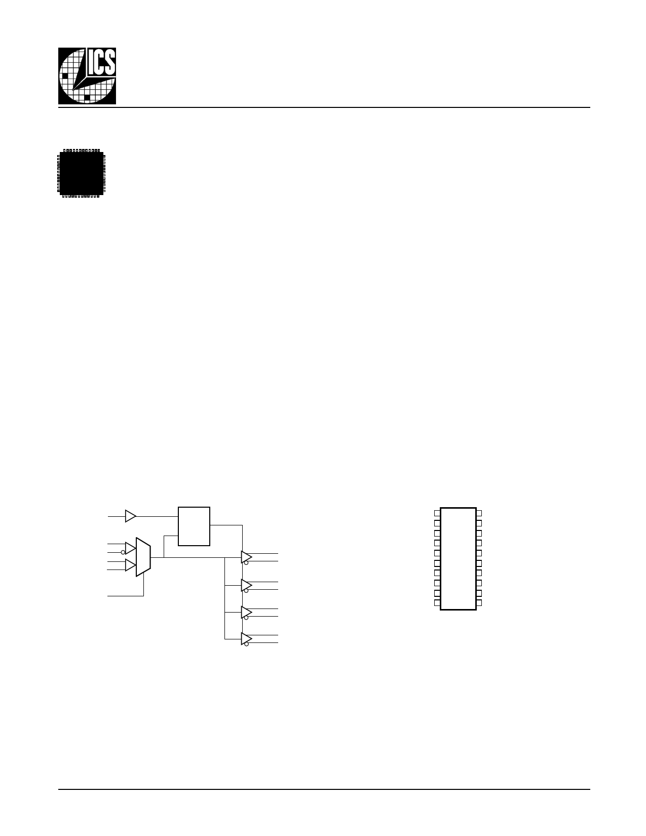
BLOCK DIAGRAM
CLK_EN
CLK
nCLK
XTAL1
XTAL2
CLK_SEL
0
1
D
Q
LE
PIN ASSIGNMENT
VEE 1
20 Q0
CLK_EN 2 19 nQ0
CLK_SEL 3
18 VCC
CLK 4 17 Q1
Q0 nCLK 5 16 nQ1
nQ0
XTAL1 6
15 Q2
XTAL2 7
14 nQ2
Q1
nc 8
13 VCC
nQ1 nc 9 12 Q3
Q2 VCC 10 11 nQ3
nQ2
ICS8533-11
Q3
nQ3
20-Lead TSSOP
6.5mm x 4.4mm x 0.92 Package Body
G Package
Top View
8533AG-11
www.icst.com/products/hiperclocks.html
1
REV. D JULY 16, 2001
1 page 
Integrated
Circuit
Systems, Inc.
ICS8533-11
LOW SKEW, 1-TO-4, CRYSTAL OSCILLATOR/
DIFFERENTIAL-TO-3.3V LVPECL FANOUT BUFFER
TABLE 4D. LVPECL DC CHARACTERISTICS, VCC = 3.3V±5%, TA = 0°C TO 70°C
Symbol
Parameter
Test Conditions Minimum
VOH Output High Voltage; NOTE 1
VOL Output Low Voltage; NOTE 1
VSWING
Peak-to-Peak Output Voltage Swing
NOTE 1: Outputs terminated with 50Ω to VCC - 2V.
VCC - 1.4
VCC - 2.0
0.6
Typical
Maximum
VCC - 1.0
VCC - 1.7
0.85
Units
V
V
V
TABLE 5. CRYSTAL CHARACTERISTICS
Parameter
Mode of Oscillation
Frequency Tolerance
Frequency Stability
Drive Level
Equivalent Series Resistance (ESR)
Shunt Capacitance
Series Pin Inductance
Operating Temperature Range
Aging
Frequency Range
Test Conditions
Per year @ 25°C
Minimum Typical Maximum
Fundamental
-50 50
-100
100
0.1
50 80
7
37
0 70
-5 5
14 25
Units
ppm
ppm
mW
Ω
pF
nH
°C
ppm
MHz
TABLE 6. AC CHARACTERISTICS, VCC = 3.3V±5%, TA = 0°C TO 70°C
Symbol Parameter
Test Conditions
Minimum Typical Maximum
fMAX
tPD
tsk(o)
Maximum Input Frequency
Propagation Delay; NOTE 1
Output Skew; NOTE 2, 5
IJ 650MHz
1.0
650
2.0
30
tsk(pp) Part-to-Part Skew; NOTE 3, 5
150
tR Output Rise Time
20% to 80% @ 50MHz
300
tF Output Fall Time
20% to 80% @ 50MHzz
300
odc Output Duty Cycle; NOTE 4
47
50
700
700
53
oscTOL Crystal Oscillator Tollerance
TBD
All parameters measured at 500MHz unless noted otherwise.
The cycle-to-cycle jitter on the input will equal the jitter on the output. The part does not add jitter.
NOTE 1: Measured from the differential input crossing point to the differential output crossing point.
NOTE 2: Defined as skew between outputs at the same supply voltage and with equal load conditions.
Measured at the output differential cross points.
NOTE 3: Defined as skew between outputs on different devices operating at the same supply voltages
and with equal load conditions. Using the same type of inputs on each device, the outputs are measured
at the differential cross points.
NOTE 4: Measured using CLK. For XTAL input, refer to Application Note.
NOTE 5: This parameter is defined in accordance with JEDEC Standard 65.
Units
MHz
ns
ps
ps
ps
ps
%
ppm
8533AG-11
www.icst.com/products/hiperclocks.html
5
REV. D JULY 16, 2001
5 Page 
Integrated
Circuit
Systems, Inc.
ICS8533-11
LOW SKEW, 1-TO-4, CRYSTAL OSCILLATOR/
DIFFERENTIAL-TO-3.3V LVPECL FANOUT BUFFER
POWER CONSIDERATIONS
This section provides information on power dissipation and junction temperature for the ICS8533-11.
Equations and example calculations are also provided.
1. Power Dissipation.
The total power dissipation for the ICS8533-11 is the sum of the core power plus the power dissipated in the load(s).
The following is the power dissipation for VCC = 3.3V + 5% = 3.465V, which gives worst case results.
NOTE: Please refer to Section 3 for details on calculating power dissipated in the load.
• Power (core)MAX = VCC_MAX * IEE_MAX = 3.465V * 50mA = 173.3mW
•
Power (outputs) = 30.2mW/Loaded Output pair
MAX
If all outputs are loaded, the total power is 4 * 30.2mW = 120.8mW
Total Power_MAX (3.465V, with all outputs switching) = 173.3mW + 120.8mW = 294.1mW
2. Junction Temperature.
Junction temperature, Tj, is the temperature at the junction of the bond wire and bond pad and directly affects the reliability of the
device. The maximum recommended junction temperature for HiPerClockSTM devices is 125°C.
The equation for Tj is as follows: Tj = θJA * Pd_total + TA
Tj = Junction Temperature
θJA = junction-to-ambient thermal resistance
Pd_total = Total device power dissipation (example calculation is in section 1 above)
TA = Ambient Temperature
In order to calculate junction temperature, the appropriate junction-to-ambient thermal resistance θJA must be used. Assuming a
moderate air flow of 200 linear feet per minute and a multi-layer board, the appropriate value is 66.6°C/W per Table 6 below.
Therefore, Tj for an ambient temperature of 70°C with all outputs switching is:
70°C + 0.294W * 66.6°C/W = 89.58°C. This is well below the limit of 125°C
This calculation is only an example. Tj will obviously vary depending on the number of loaded outputs, supply voltage, air flow,
and the type of board (single layer or multi-layer).
Table 7. Thermal Resistance qJA for 20-pin TSSOP, Forced Convection
qJA by Velocity (Linear Feet per Minute)
0
Single-Layer PCB, JEDEC Standard Test Boards 114.5°C/W
Multi-Layer PCB, JEDEC Standard Test Boards 73.2°C/W
200
98.0°C/W
66.6°C/W
500
88.0°C/W
63.5°C/W
NOTE: Most modern PCB designs use multi-layered boards. The data in the second row pertains to most designs.
8533AG-11
www.icst.com/products/hiperclocks.html
11
REV. D JULY 16, 2001
11 Page | ||
| Páginas | Total 15 Páginas | |
| PDF Descargar | [ Datasheet ICS8533-11.PDF ] | |
Hoja de datos destacado
| Número de pieza | Descripción | Fabricantes |
| ICS8533-11 | LVPECL FANOUT BUFFER | ICST |
| Número de pieza | Descripción | Fabricantes |
| SLA6805M | High Voltage 3 phase Motor Driver IC. |
Sanken |
| SDC1742 | 12- and 14-Bit Hybrid Synchro / Resolver-to-Digital Converters. |
Analog Devices |
|
DataSheet.es es una pagina web que funciona como un repositorio de manuales o hoja de datos de muchos de los productos más populares, |
| DataSheet.es | 2020 | Privacy Policy | Contacto | Buscar |