|
|
|
PDF IR3621 Data sheet ( Hoja de datos )
| Número de pieza | IR3621 | |
| Descripción | 2-PHASE / DUAL SYNCHRONOUS PWM CONTROLLER | |
| Fabricantes | International Rectifier | |
| Logotipo | ||
Hay una vista previa y un enlace de descarga de IR3621 (archivo pdf) en la parte inferior de esta página. Total 29 Páginas | ||
|
No Preview Available !
www.DataSheet4U.com
Data Sheet No.PD60231 revA
IR3621 & (PbF)
2-PHASE / DUAL SYNCHRONOUS PWM CONTROLLER WITH
OSCILLATOR SYNCHRONIZATION AND PRE-BIAS STARTUP
FEATURES
Dual Synchronous Controller with 180!
Out of Phase Operation
Configurable to 2-Independent Outputs or
Current Share Single Output
Voltage Mode Control
Current Sharing Using Inductor's DCR
Selectable Hiccup or Latched Current
Limit using MOSFET's RDS(on) sensing
Latched Over-Voltage Protection
Pre-Bias Start Up
Programmable Switching Frequency up to 500KHz
Two Independent Soft-Starts/Shutdowns
Precision Reference Voltage 0.8V
Power Good Output
External Frequency Synchronization
Thermal Protection
APPLICATIONS
Embedded Networking & Telecom Systems
Distributed Point-of-Load Power Architectures
2-Phase Power Supply
Graphics Card
DDR Memory Applications
DESCRIPTION
The IR3621 IC combines a dual synchronous buck control-
ler and drivers, providing a cost-effective, high performance
and flexible solution. The IR3621 operates in 2-Phase mode
to produce either 2-independent output voltages or current
share single output for high current application. The 180!
out-of-phase operation allows the reduction of input and
output capacitance.
Other key features include two independently programmable
soft-start functions to allow system level sequencing of out-
put voltages in various configurations. The pre-bias protec-
tion feature prevents the discharge of the output voltage and
possible damage to the load during start-up when a pre-
existing voltage is present at the output. Programmable
switching frequency up to 500KHz per phase allows flexibil-
ity to tune the operation of the IC to meet system level re-
quirements, and synchronization allows the simplification
of system level filter design. Protection features such as
selectable hiccup or latched current limit, and under voltage
lock-out are provided to give required system level security
in the event of a fault condition.
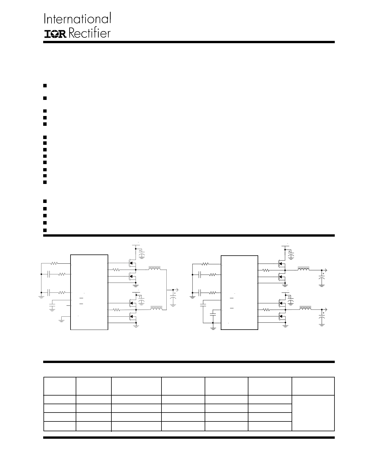
Vin Vin
Rt
Comp1
HDrv1
OCSet1
LDrv1
PGnd1
Comp2 IR3621
SS1 / SD
SS2 / SD
Gnd
HDrv2
OCSet2
LDrv2
PGnd2
Vin
Rt
Comp1
HDrv1
OCSet1
LDrv1
PGnd1
Vout
Comp2 IR3621
Vin
SS1 / SD
SS2 / SD
Gnd
HDrv2
OCSet2
LDrv2
PGnd2
Vout1
Vout2
Current share, single output configuration
2-independent output voltage configuration
Figure 1 - Typical application of IR3621 in current share single output and 2-independent output voltage configuration
PKG
DESIG
M
M
F
F
ORDERING INFORMATION
PART
NUMBER
IR3621M
IR3621MTR
IR3621F
IR3621FTR
LEADFREE
PART NUMBER
IR3621MPbF
IR3621MTRPbF
N/A
N/A
PIN
COUNT
32
32
28
28
PARTS
PER TUBE
73
------
50
------
PARTS
PER REEL
------
6000
------
2500
T&R
Orientation
Fig A
www.irf.com
1
1 page 
IR3621 & (PbF)
PIN DESCRIPTIONS
TSSOP
1
2
3
4
5,23
6,22
7,21
8
20
9,19
10,18
11,17
12,16
13,15
14
24
25
26
27
28
MLPQ PIN SYMBOL PIN DESCRIPTION
29 PGood Power Good pin. Low when any of the outputs fall 10% below the set voltages.
30 Vcc Supply voltage for the internal blocks of the IC. The Vcc slew rate should be
<0.1V/us.
31
VOUT3
Output of the internal LDO. Connect a 1.0uF capacitor from this pin to ground.
1 Rt Connecting a resistor from this pin to ground sets the oscillator frequency.
2,22 VSEN2, VSEN1 Sense pins for OVP and PGood. For current share tie these pins together.
3,21 Fb2,Fb1 Inverting inputs to the error amplifiers. In current sharing mode, Fb1 is con-
nected to a resistor divider to set the output voltage and Fb2 is connected to
programming resistor to achieve current sharing. In independent 2-channel mode,
these pins work as feedback inputs for each channel.
4,20 Comp2, Comp1 Compensation pins for the error amplifiers.
5 SS2 / SD These pins provide user programmable soft-start function for each outputs.
19 SS1 / SD Connect external capacitors from these pins to ground to set the start up time
for each output. These outputs can be shutdown independently by pulling the
respective pins below 0.3V. During shutdown both MOSFETs will be turned off.
For current share mode SS2 must be floating.
6,18 OCSet2,OCSet1 A resistor from these pins to switching point will set current limit threshold.
7,17 VcH2, VcH1 Supply voltage for the high side output drivers. These are connected to voltages
that must be typically 6V higher than their bus voltages. A 0.1µF high fre-
quency capacitor must be connected from these pins to PGND to provide peak
drive current capability.
8,16 HDrv2, HDrv1 Output drivers for the high side power MOSFETs. Note3
10,14 PGnd2, PGnd1 These pins serve as the separate grounds for MOSFET drivers and should be
connected to the system’s ground plane.
11,13 LDrv2, LDrv1 Output drivers for the synchronous power MOSFETs.
12 VCL Supply voltage for the low side output drivers.
23
Sync
The internal oscillator can be synchronized to an external clock via this pin.
24 Hiccup When pulled High, it puts the device current limit into a hiccup mode. When
pulled Low, the output latches off, after an overcurrent event.
26 VP2 Non-inverting input to the second error amplifier. In the current sharing mode, it
is connected to the programming resistor to achieve current sharing. In inde-
pendent 2-channel mode it is connected to VREF pin when Fb2 is connected to
the resistor divider to set the output voltage.
27 VREF Reference Voltage. The drive capability of this pin is about 2µA.
28 Gnd Analog ground for internal reference and control circuitry.
9,15,25.32
N/C
No Connect
Note3: The negative voltage at these pins may cause instability for the gate drive circuits. To prevent this, a low
forward voltage drop diode (Schottky) is required between these pins and power ground.
www.irf.com
5
5 Page 
IR3621 & (PbF)
APPLICATION INFORMATION
Design Example:
The following example is a typical application for the
IR3621, the schematic is Figure19 on page18.
VIN = 12V
VOUT(2.5V) = 2.5V @ 10A
VOUT(1.8V) = 1.8V @ 10A
∆VOUT = Output voltage ripple ≅ 3% of VOUT
FS = 400kHz
Output Voltage Programming
Output voltage is programmed by the reference voltage
and an external voltage divider. The Fb1 pin is the invert-
ing input of the error amplifier, which is referenced to the
voltage on the non-inverting pin of error amplifier. For this
application, this pin (VP2) is connected to the reference
voltage (VREF). The output voltage is defined by using the
following equation:
( )VOUT = VP2 ×
1
+
R6
R5
---(4)
VP2 = VREF = 0.8V
When an external resistor divider is connected to the
output as shown in Figure 11.
VOUT
IR3621
VREF
VP2
Fb
R6
R5
Figure 11 - Typical application of the IR3621 for pro-
gramming the output voltage.
Equation (4) can be rewritten as:
( )R6 = R5 ×
VOUT
VP
-1
Will result to:
VOUT(2.5V) = 2.5V
VREF = 0.8V
R9= 2.15K, R5= 1K
VOUT(1.8V) = 1.8V
VREF = 0.8
R7= 1.24K, R8 = 1K
If the high value feedback resistors are used, the input
bias current of the Fb pin could cause a slight increase
in output voltage. The output voltage can be set more
accurately by using low value, precision resistors.
Soft-Start Programming
The soft-start timing can be programmed by selecting
the soft-start capacitance value. The start-up time of
the converter can be calculated by using:
Css ≅ 28×tSTART (µF) ---(5)
Where tSTART is the desired start-up time (ms)
For a start-up time of 4ms for both output, the soft-start
capacitor will be 0.1µF. Connect two 0.1µFceramic
capacitors from SS1 pin and SS2 pin to GND.
Supply VcH1 and VcH2
To drive the high side MOSFET, it is necessary to sup-
ply a gate voltage at least 4V greater than the bus volt-
age. This is achieved by using a charge pump configu-
ration as shown in Figure 12. This method is simple
and inexpensive. The operation of the circuit is as fol-
lows: when the lower MOSFET is turned on, the ca-
pacitor (C1) charges up to VOUT3, through the diode
(D1). The bus voltage will be added to this voltage when
upper MOSFET turns on in next cycle, and providing
supply voltage (VcH1) through diode (D2). VcH1 is ap-
proximately:
VCH1 ≅ VOUT3 + VBUS - (VD1 + VD2)
Capacitor in the range of 0.1µF is generally adequate
for most applications. The diode must be a fast recov-
ery device to minimize the amount of charge fed back
from the charge pump capacitor into VOUT3. The diodes
need to be able to block the full power rail voltage, which
is seen when the high side MOSFET is switched on.
For low voltage application, Schottky diodes can be
used to minimize forward drop across the diodes at
start up.
VOUT3
D1
C3
D2
Regulator
VcH1
VBUS
C2 C1
Q1
L2
IR3621 HDrv Q2
Figure 12 - Charge pump circuit.
www.irf.com
11
11 Page | ||
| Páginas | Total 29 Páginas | |
| PDF Descargar | [ Datasheet IR3621.PDF ] | |
Hoja de datos destacado
| Número de pieza | Descripción | Fabricantes |
| IR3621 | 2-PHASE / DUAL SYNCHRONOUS PWM CONTROLLER | International Rectifier |
| IR3621PBF | 2-PHASE / DUAL SYNCHRONOUS PWM CONTROLLER | International Rectifier |
| IR3622AMPBF | SINGLE OR DUAL OUTPUT SYNCHRONOUS STEP DOWN CONTROLLER | International Rectifier |
| IR3622MPBF | SINGLE OR DUAL OUTPUT SYNCHRONOUS STEP DOWN CONTROLLER | International Rectifier |
| Número de pieza | Descripción | Fabricantes |
| SLA6805M | High Voltage 3 phase Motor Driver IC. |
Sanken |
| SDC1742 | 12- and 14-Bit Hybrid Synchro / Resolver-to-Digital Converters. |
Analog Devices |
|
DataSheet.es es una pagina web que funciona como un repositorio de manuales o hoja de datos de muchos de los productos más populares, |
| DataSheet.es | 2020 | Privacy Policy | Contacto | Buscar |