|
|
|
PDF GM7230 Data sheet ( Hoja de datos )
| Número de pieza | GM7230 | |
| Descripción | 3A STEP-DOWN VOLTAGE REGULATOR | |
| Fabricantes | Gamma | |
| Logotipo | ||
Hay una vista previa y un enlace de descarga de GM7230 (archivo pdf) en la parte inferior de esta página. Total 12 Páginas | ||
|
No Preview Available !
www.DataSheet4U.com
GM7230
3A STEP-DOWN VOLTAGE REGULATOR
Power Management
Description
The GM7230 series of regulators provide all the active func-
tions for a step-down (buck) switching regulator, and drive
3A load with excellent line and load regulation. GM7230's
are available in fixed output voltages of 3.3V, 5V, 12V, and
a versatile Adjustable output version.
These regulators are simple to use and require a minimum
number of external components. Features include internal
frequency compensation and a fixed-frequency oscillator.
The GM7230 series are high-efficiency replacements for
popular three-terminal linear regulators, requiring a smaller
heatsink or even no heatsink.
The GM7230's perform well with standard inductors from
several manufacturers, simplifying the design of switch-
mode power supplies. The GM7230 series guarantee ±4%
tolerance on output voltage within specified input voltages
and output load conditions, and ±10% on the oscillator fre-
quency.
Features
3.3V, 5V, 12V and Adjustable output versions
Adjustable version output voltage range 1.23V
to 37V 4% max over line and load conditions
3A output current
Input voltage range up to 40V
Requires only 4 external components
High efficiency
TTL shutdown capability, low power standby
mode
Thermal shutdown, current limit protection
Uses standard inductors
150 kHz fixed frequency internal oscillator
External shutdown is included, with 80 µA (typical) standby
current. The output switch has cycle-by-cycle current limit-
ing, as well as thermal shutdown for full protection under
fault conditions.
Application
Pre-regulator for linear regulators
On-card/board switching regulators
High-efficiency step-down buck regulator Positive to negative converter (buck-boost)
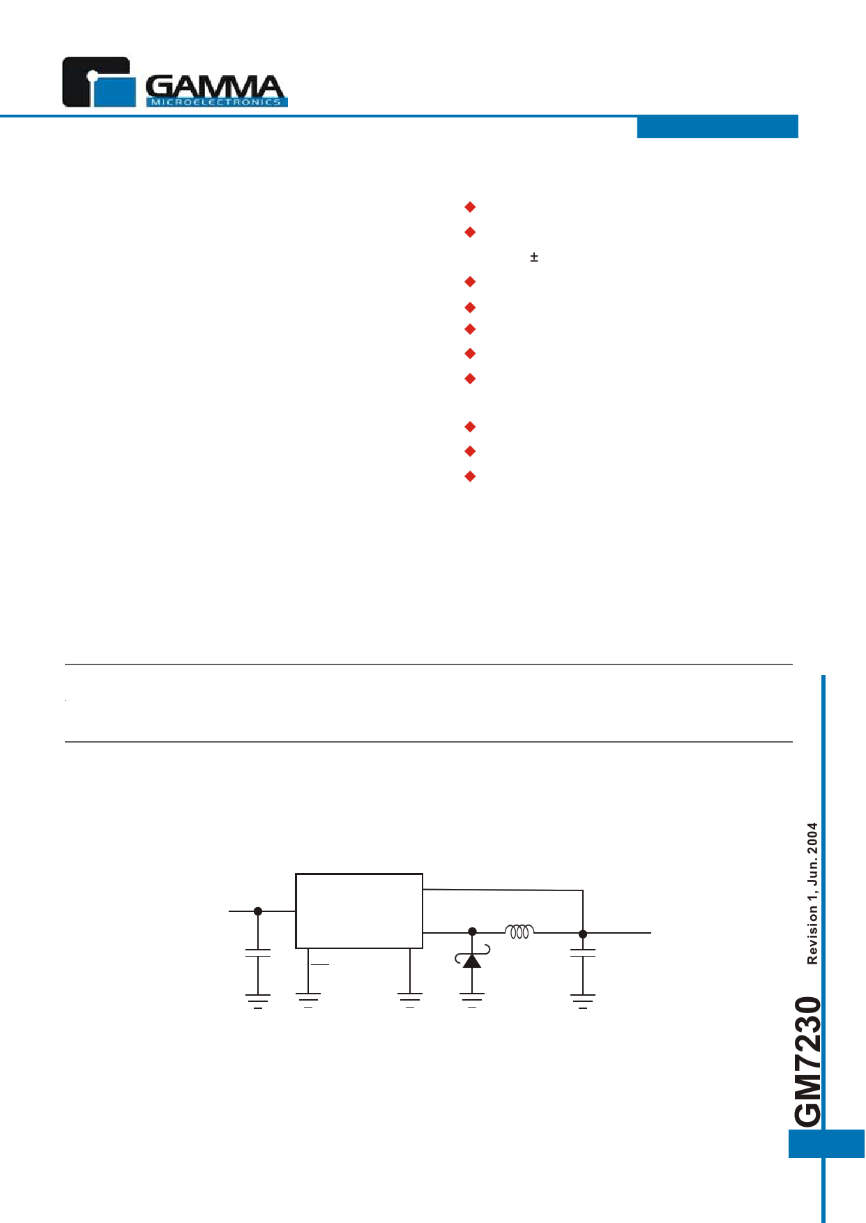
TYPICAL APPLICATIONS
12V
Unregulated
DC Input
+VIN GM7230
1 5.0
+ CIN
5
680 µF ON / OFF
Feedback
4
Output
2
L1
3
GND
68 µH
D1
1N5824
5.0V
Regulated
+
Output
COUT 3A Load
220 µF
www.gammamicro.com 1
PRELIMINARY
1 page 
GM7230
ELECTRICAL CHARACTERISTICS: All Output Voltage Versions
(Specifications with standard type face are for TJ = 25 C, and those with boldface type apply over full Operating Temperature Range.
Unless otherwise specified, VIN= 12V for the 3.3V, 5.0V and ADJ version and VIN= 24V for 12V version. ILOAD = 500 mA)
Parameter
Conditions
Symbol Min
Typ
Max
Feedback Bias Current
Oscillator Frequency
VFB = 1.3V (Adjustable Version Only)
(Note 6)
Saturation Voltage
Max Duty Cycle (ON)
IOUT = 3A (Notes 7, 8)
(Note 8)
Min Duty Cycle (OFF)
(Note 9)
Current Limit
Output Leakage Current
Quiescent Current
Peak Current (Notes 7, 8)
(Notes 7, 9, 10)
(Notes 10)
Output = 0 V
Output = -1V
(Note 9)
Standby Quiescent Current ON/OFF Pin = 5V (OFF) (Note 10)
Thermal Resistance
TO-220 or TO-263 Package, Junction to Case
TO-220 Package, Junction to Ambient (Note 11)
TO-263 Package, Junction to Ambient (Note 12)
TO-263 Package, Junction to Ambient (Note 13)
TO-263 Package, Junction to Ambient (Note 14)
ON/OFF Pin
Low (ON)
Logic Input Level
High (OFF)
ON/OFF Pin Input Current
VLOGIC = 2.5V (OFF)
VLOGIC = 0.5V (ON)
Ib
fo
VSAT
DC
DC
ICL
IL
IQ
ISTBY
qJC
qJA
qJA
qJA
qJA
VIH
VIL
IH
IL
-
127/110
-
3.6 / 3.4
-
-
-
-
-
-
-
-
-
-
2.0
-
-
10
150
1.16
100
0
4.5
-
2
5
80
2
50
50
30
20
1.3
1.3
5
0.02
50 / 100
173 / 173
1.4 / 1.5
-
-
6.9 / 7.5
50
30
10
200 / 250
-
-
-
-
-
0.6
-
15
5
Unit
nA
kHz
V
%
%
A
µA
mA
mA
µA
°C/W
V
V
µA
µA
Note 1: Absolute Maximum Ratings indicate limits beyond which damage to the device may occur. Operating Ratings indicate conditions for which the device is
intended to be functional, but do not guarantee specific performance limits. For guaranteed specifications and test conditions, see the Electrical
Characteristics.
Note 2: The human body model is a 100 pF capacitor discharged through a 1.5k resistor into each pin.
Note 3: Typical numbers are at 25°C and represent the most likely norm.
Note 4: All limits guaranteed at room temperature (standard type face) and at temperature extremes (bold type face). All room temperature limits are
100% production tested. All limits at temperature extremes are guaranteed via correlation using standard Statistical Quality Control (SQC) methods.
All limits are used to calculate Average Outgoing Quality Level (AOQL).
Note 5: External components such as the catch diode, inductor, input and output capacitors, and voltage programming resistors can affect switching regulator
system performance. When the GM7230 is used as shown in the Figure 1 test circuit, system performance will be as shown in system parameters section
of Electrical Characteristics.
Note 6: The switching frequency is reduced when the second stage current limit is activated.
Note 7: No diode, inductor or capacitor connected to output pin.
Note 8: Feedback pin removed from output and connected to 0V to force the output transistor switch ON.
Note 9: Feedback pin removed from output and connected to 12V for the 3.3V, 5V, and the ADJ. version, and 15V for the 12V version, to force the output transistor
switch OFF.
Note 10: VIN = 40V.
Note 11: Junction to ambient thermal resistance (no external heat sink) for the TO-220 package mounted vertically, with the leads soldered to a printed circuit board
with (1 oz.) copper area of approximately 1 in2.
Note 12: Junction to ambient thermal resistance with the TO-263 package tab soldered to a single printed circuit board with 0.5 in2 of (1 oz.) copper area.
Note 13: Junction to ambient thermal resistance with the TO-263 package tab soldered to a single sided printed circuit board with 2.5 in2 of (1 oz.) copper area.
Note 14: Junction to ambient thermal resistance with the TO-263 package tab soldered to a double sided printed circuit board with 3 in2 of (1 oz.) copper area on
the GM7230 side of the board, and approximately 16 in2 of copper on the other side of the p-c board.
5
5 Page 
TO-220-5 PACKAGE OUTLINE DIMENSIONS
3.60 ± 0.20
1.30 ± 0.10
1.70
1.50 DP0.20
1.2
9.90 ± 0.20
8.70
2.80 ± 0.10
4.50 ± 0.20
1.30
+0.1
-0.05
3.70 ± 0.20
4.60
8.40
P3°
7.0 ± 0.20
9.20 ± 0.20
3° 3°
3-R0.2
9.97 ± 0.20
8.0 ± 0.20
7.0
GM7230
1.7(TYP)
3°
5-0.8 ± 0.10
3°
2 - R 0.3
0.50
+0.1
-0.05
2.40 ± 0.20
10.00 ± 0.20
Unit: mm
TO-263-5 PACKAGE OUTLINE DIMENSIONS
0.40
4.60
9.90
15°
1.20
1.50 DP0.20
9.20
4.50
1.30
3°
1.20
1.70 TYP
(1.70 ± 0.20)
3°
R 0.3
15.3
P4.90
0.80
2.00
0.75
R0.30
0.40
10.0
8.0
7.0
4.40
0.10
3°
2.40
R0.30
2.54
0.50
1.75
3°
0.90
R 0.45
7.2
9.20
10.00
15.30
Pad Layout
17.5
9
4.90
Unit: mm
3.8
1.7
1.07
Units: mm
11
11 Page | ||
| Páginas | Total 12 Páginas | |
| PDF Descargar | [ Datasheet GM7230.PDF ] | |
Hoja de datos destacado
| Número de pieza | Descripción | Fabricantes |
| GM7230 | 3A STEP-DOWN VOLTAGE REGULATOR | Gamma |
| Número de pieza | Descripción | Fabricantes |
| SLA6805M | High Voltage 3 phase Motor Driver IC. |
Sanken |
| SDC1742 | 12- and 14-Bit Hybrid Synchro / Resolver-to-Digital Converters. |
Analog Devices |
|
DataSheet.es es una pagina web que funciona como un repositorio de manuales o hoja de datos de muchos de los productos más populares, |
| DataSheet.es | 2020 | Privacy Policy | Contacto | Buscar |