|
|
|
PDF SC1100 Data sheet ( Hoja de datos )
| Número de pieza | SC1100 | |
| Descripción | Information Appliance On a Chip | |
| Fabricantes | National Semiconductor | |
| Logotipo | ||
Hay una vista previa y un enlace de descarga de SC1100 (archivo pdf) en la parte inferior de esta página. Total 70 Páginas | ||
|
No Preview Available !
www.DataSheet4U.com
March 2003
Revision 1.1
Geode™ SC1100
Information Appliance On a Chip
General Description
The Geode™ SC1100 device is a member of the National
Semiconductor® Information Appliance On a Chip (IAOC)
family of fully integrated x86 system chips. The main mod-
ules of the Geode SC1100 are:
• Geode GX1 processor module - Combines advanced
CPU performance with Intel MMX support, a 64-bit
synchronous DRAM (SDRAM) interface, and a PCI bus
controller.
• Core Logic module - Includes PC/AT functionality, a USB
interface, an IDE interface, a PCI bus interface, an LPC
bus interface, Advanced Configuration Power Interface
(ACPI) version 1.0 compliant power management, and
an audio codec interface.
• SuperI/O module - Has a Serial Port (UART), an Infrared
(IR) interface, two ACCESS.bus (ACB) interfaces, and a
Real-Time Clock (RTC).
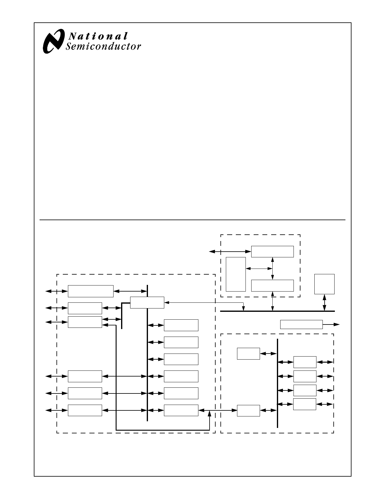
The block diagram shows the relationships between the
modules.
These features, combined with the device’s small form fac-
tor and low power consumption, make it ideal as the core
for an advanced set-top box, consumer access device, res-
idential gateway, thin client, or embedded system.
Block Diagram
IDE I/F
USB
PCI/Sub-ISA
Bus I/F
GPIO
Audio Codec I/F
LPC I/F
Fast X-Bus
Core Logic
Bridge
PIT
PIC
DMAC
Pwr Mgmnt
Configuration
X-Bus
ISA Bus I/F
Geode™ GX1
Memory Controller
CPU
Core
PCI Bus
Controller
Config.
Block
Fast-PCI Bus
Clock & Reset Logic
RTC
SuperI/O
ISA Bus
I/F
ACB1
I/F
ACB2
I/F
UART
IR
National Semiconductor and Virtual System Architecture are registered trademarks of National Semiconductor Corporation.
Geode and VSA are trademarks of National Semiconductor Corporation.
For a complete listing of National Semiconductor trademarks, please visit www.national.com/trademarks.
© 2003 National Semiconductor Corporation
www.national.com
1 page 
Table of Contents (Continued)
3.0 General Configuration Block . . . . . . . . . . . . . . . . . . . . . . . . . . . . . . . . . . . . . . . . 49
3.1 CONFIGURATION BLOCK ADDRESSES . . . . . . . . . . . . . . . . . . . . . . . . . . . . . . . . . . . . . . . . 49
3.2 MULTIPLEXING, INTERRUPT SELECTION, AND BASE ADDRESS REGISTERS . . . . . . . . 50
3.3 WATCHDOG . . . . . . . . . . . . . . . . . . . . . . . . . . . . . . . . . . . . . . . . . . . . . . . . . . . . . . . . . . . . . . . 55
3.3.1 Functional Description . . . . . . . . . . . . . . . . . . . . . . . . . . . . . . . . . . . . . . . . . . . . . . . . 55
3.3.1.1 WATCHDOG Timer . . . . . . . . . . . . . . . . . . . . . . . . . . . . . . . . . . . . . . . . . . . . . . . . 55
3.3.2 WATCHDOG Registers . . . . . . . . . . . . . . . . . . . . . . . . . . . . . . . . . . . . . . . . . . . . . . . 56
3.3.2.1 Usage Hints . . . . . . . . . . . . . . . . . . . . . . . . . . . . . . . . . . . . . . . . . . . . . . . . . . . . . . 56
3.4 HIGH-RESOLUTION TIMER . . . . . . . . . . . . . . . . . . . . . . . . . . . . . . . . . . . . . . . . . . . . . . . . . . 57
3.4.1 Functional Description . . . . . . . . . . . . . . . . . . . . . . . . . . . . . . . . . . . . . . . . . . . . . . . . 57
3.4.2 High-Resolution Timer Registers . . . . . . . . . . . . . . . . . . . . . . . . . . . . . . . . . . . . . . . . 57
3.4.2.1 Usage Hints . . . . . . . . . . . . . . . . . . . . . . . . . . . . . . . . . . . . . . . . . . . . . . . . . . . . . . 57
3.5 CLOCK GENERATORS AND PLLS . . . . . . . . . . . . . . . . . . . . . . . . . . . . . . . . . . . . . . . . . . . . . 59
3.5.1
3.5.2
3.5.3
3.5.4
3.5.5
3.5.6
27 MHz Crystal Oscillator . . . . . . . . . . . . . . . . . . . . . . . . . . . . . . . . . . . . . . . . . . . . . . 60
GX1 Module Core Clock . . . . . . . . . . . . . . . . . . . . . . . . . . . . . . . . . . . . . . . . . . . . . . . 61
Internal Fast-PCI Clock . . . . . . . . . . . . . . . . . . . . . . . . . . . . . . . . . . . . . . . . . . . . . . . 61
SuperI/O Clocks . . . . . . . . . . . . . . . . . . . . . . . . . . . . . . . . . . . . . . . . . . . . . . . . . . . . . 62
Core Logic Module Clocks . . . . . . . . . . . . . . . . . . . . . . . . . . . . . . . . . . . . . . . . . . . . . 62
Clock Registers . . . . . . . . . . . . . . . . . . . . . . . . . . . . . . . . . . . . . . . . . . . . . . . . . . . . . 63
4.0 SuperI/O Module . . . . . . . . . . . . . . . . . . . . . . . . . . . . . . . . . . . . . . . . . . . . . . . . . . 65
4.1 FEATURES . . . . . . . . . . . . . . . . . . . . . . . . . . . . . . . . . . . . . . . . . . . . . . . . . . . . . . . . . . . . . . . 66
4.2 MODULE ARCHITECTURE . . . . . . . . . . . . . . . . . . . . . . . . . . . . . . . . . . . . . . . . . . . . . . . . . . . 67
4.3 CONFIGURATION STRUCTURE / ACCESS . . . . . . . . . . . . . . . . . . . . . . . . . . . . . . . . . . . . . 68
4.3.1
4.3.2
4.3.3
4.3.4
Index-Data Register Pair . . . . . . . . . . . . . . . . . . . . . . . . . . . . . . . . . . . . . . . . . . . . . . 68
Banked Logical Device Registers . . . . . . . . . . . . . . . . . . . . . . . . . . . . . . . . . . . . . . . . 68
Default Configuration Setup . . . . . . . . . . . . . . . . . . . . . . . . . . . . . . . . . . . . . . . . . . . . 69
Address Decoding . . . . . . . . . . . . . . . . . . . . . . . . . . . . . . . . . . . . . . . . . . . . . . . . . . . 69
4.4 STANDARD CONFIGURATION REGISTERS . . . . . . . . . . . . . . . . . . . . . . . . . . . . . . . . . . . . . 70
4.4.1 SIO Control and Configuration Registers . . . . . . . . . . . . . . . . . . . . . . . . . . . . . . . . . . 73
4.4.2 Logical Device Control and Configuration . . . . . . . . . . . . . . . . . . . . . . . . . . . . . . . . . 74
4.4.2.1
4.4.2.2
LDN 00h - Real-Time Clock . . . . . . . . . . . . . . . . . . . . . . . . . . . . . . . . . . . . . . . . . 74
LDN 01h - System Wakeup Control . . . . . . . . . . . . . . . . . . . . . . . . . . . . . . . . . . . 76
4.4.2.3
4.4.2.4
LDN 02h - Infrared Communication Port . . . . . . . . . . . . . . . . . . . . . . . . . . . . . . . . 77
LDN 05h and 06h - ACCESS.bus Ports 1 and 2 . . . . . . . . . . . . . . . . . . . . . . . . . . 78
4.4.2.5 LDN 08h - SP Configuration . . . . . . . . . . . . . . . . . . . . . . . . . . . . . . . . . . . . . . . . . 79
4.5 REAL-TIME CLOCK (RTC) . . . . . . . . . . . . . . . . . . . . . . . . . . . . . . . . . . . . . . . . . . . . . . . . . . . 80
4.5.1
4.5.2
4.5.3
4.5.4
4.5.5
Bus Interface . . . . . . . . . . . . . . . . . . . . . . . . . . . . . . . . . . . . . . . . . . . . . . . . . . . . . . . 80
RTC Clock Generation . . . . . . . . . . . . . . . . . . . . . . . . . . . . . . . . . . . . . . . . . . . . . . . . 80
4.5.2.1 Internal Oscillator . . . . . . . . . . . . . . . . . . . . . . . . . . . . . . . . . . . . . . . . . . . . . . . . . 80
4.5.2.2 External Oscillator . . . . . . . . . . . . . . . . . . . . . . . . . . . . . . . . . . . . . . . . . . . . . . . . . 81
Timing Generation . . . . . . . . . . . . . . . . . . . . . . . . . . . . . . . . . . . . . . . . . . . . . . . . . . . 81
4.5.3.1 Timekeeping . . . . . . . . . . . . . . . . . . . . . . . . . . . . . . . . . . . . . . . . . . . . . . . . . . . . . 82
4.5.3.2 Alarms . . . . . . . . . . . . . . . . . . . . . . . . . . . . . . . . . . . . . . . . . . . . . . . . . . . . . . . . . . 82
4.5.3.3 Power Supply . . . . . . . . . . . . . . . . . . . . . . . . . . . . . . . . . . . . . . . . . . . . . . . . . . . . 83
4.5.3.4 System Power States . . . . . . . . . . . . . . . . . . . . . . . . . . . . . . . . . . . . . . . . . . . . . . 84
4.5.3.5 Oscillator Activity . . . . . . . . . . . . . . . . . . . . . . . . . . . . . . . . . . . . . . . . . . . . . . . . . . 84
4.5.3.6 Interrupt Handling . . . . . . . . . . . . . . . . . . . . . . . . . . . . . . . . . . . . . . . . . . . . . . . . . 85
4.5.3.7 Battery-Backed RAMs and Registers . . . . . . . . . . . . . . . . . . . . . . . . . . . . . . . . . . 85
RTC Registers . . . . . . . . . . . . . . . . . . . . . . . . . . . . . . . . . . . . . . . . . . . . . . . . . . . . . . 86
4.5.4.1 Usage Hints . . . . . . . . . . . . . . . . . . . . . . . . . . . . . . . . . . . . . . . . . . . . . . . . . . . . . . 91
RTC General-Purpose RAM Map . . . . . . . . . . . . . . . . . . . . . . . . . . . . . . . . . . . . . . . . 91
Revision 1.1
5 www.national.com
5 Page 
Architecture Overview (Continued)
1.1.1 Integer Unit
The integer unit consists of:
• Instruction Buffer
• Instruction Fetch
• Instruction Decoder and Execution
The pipelined integer unit fetches, decodes, and executes
x86 instructions through the use of a five-stage integer
pipeline.
The instruction fetch pipeline stage generates, from the on-
chip cache, a continuous high-speed instruction stream for
use by the module. Up to 128 bits of code are read during a
single clock cycle.
Branch prediction logic within the prefetch unit generates a
predicted target address for unconditional or conditional
branch instructions. When a branch instruction is detected,
the instruction fetch stage starts loading instructions at the
predicted address within a single clock cycle. Up to 48
bytes of code are queued prior to the instruction decode
stage.
The instruction decode stage evaluates the code stream
provided by the instruction fetch stage and determines the
number of bytes in each instruction and the instruction
type. Instructions are processed and decoded at a maxi-
mum rate of one instruction per clock.
The address calculation function is pipelined and contains
two stages, AC1 and AC2. If the instruction refers to a
memory operand, AC1 calculates a linear memory address
for the instruction.
The AC2 stage performs any required memory manage-
ment functions, cache accesses, and register file
accesses. If a floating point instruction is detected by AC2,
the instruction is sent to the floating point unit for process-
ing.
The execution stage, under control of microcode, executes
instructions using the operands provided by the address
calculation stage.
Write-back, the last stage of the integer unit, updates the
register file within the integer unit or writes to the load/store
unit within the memory management unit.
1.1.2 Floating Point Unit
The floating point unit (FPU) interfaces to the integer unit
and the cache unit through a 64-bit bus. The FPU is x87-
instruction-set compatible and adheres to the IEEE-754
standard. Because almost all applications that contain FPU
instructions also contain integer instructions, the GX1 mod-
ule’s FPU achieves high performance by completing inte-
ger and FPU operations in parallel.
FPU instructions are dispatched to the pipeline within the
integer unit. The address calculation stage of the pipeline
checks for memory management exceptions and accesses
memory operands for use by the FPU. Once the instruc-
tions and operands have been provided to the FPU, the
FPU completes instruction execution independently of the
integer unit.
1.1.3 Write-Back Cache Unit
The 16 KB write-back unified (data/instruction) cache is
configured as four-way set associative. The cache stores
up to 16 KB of code and data in 1024 cache lines.
The GX1 module provides the ability to allocate a portion of
the L1 cache as a scratchpad, which is used to accelerate
the Virtual Systems Architecture technology algorithms.
1.1.4 Memory Management Unit
The memory management unit (MMU) translates the linear
address supplied by the integer unit into a physical address
to be used by the cache unit and the internal bus interface
unit. Memory management procedures are x86-compati-
ble, adhering to standard paging mechanisms.
The MMU also contains a load/store unit that is responsible
for scheduling cache and external memory accesses. The
load/store unit incorporates two performance-enhancing
features:
• Load-store reordering that gives memory reads,
required by the integer unit, priority over writes to
external memory.
• Memory-read bypassing that eliminates unnecessary
memory reads by using valid data from the execution
unit.
1.1.5 Internal Bus Interface Unit
The internal bus interface unit provides a bridge from the
GX1 module to the integrated system functions and the
Fast-PCI bus interface.
When an external memory access is required, the physical
address is calculated by the memory management unit and
then passed to the internal bus interface unit, which trans-
lates the cycle to an X-Bus cycle (the X-Bus is a proprietary
internal bus which provides a common interface for all of
the integrated functions). The X-Bus memory cycle is arbi-
trated between other pending X-Bus memory requests to
the SDRAM controller before completing.
In addition, the internal bus interface unit provides configu-
ration control for up to 20 different regions within system
memory with separate controls for read access, write
access, cacheability, and PCI access.
Revision 1.1
11 www.national.com
11 Page | ||
| Páginas | Total 70 Páginas | |
| PDF Descargar | [ Datasheet SC1100.PDF ] | |
Hoja de datos destacado
| Número de pieza | Descripción | Fabricantes |
| SC1100 | Information Appliance On a Chip | National Semiconductor |
| SC11004 | 300 / 1200 Bit Per Second Modem | ETC |
| SC11006 | 2400-Bit Per Second Modem Analog Peripheral | Sierra Semiconductor |
| SC1101 | Asynchronous Voltage Mode PWM Controller | Semtech Corporation |
| Número de pieza | Descripción | Fabricantes |
| SLA6805M | High Voltage 3 phase Motor Driver IC. |
Sanken |
| SDC1742 | 12- and 14-Bit Hybrid Synchro / Resolver-to-Digital Converters. |
Analog Devices |
|
DataSheet.es es una pagina web que funciona como un repositorio de manuales o hoja de datos de muchos de los productos más populares, |
| DataSheet.es | 2020 | Privacy Policy | Contacto | Buscar |