|
|
|
PDF SCF5742 Data sheet ( Hoja de datos )
| Número de pieza | SCF5742 | |
| Descripción | (SCF5740 - SCF5744) Dot Addressable Intelligent Display | |
| Fabricantes | Siemens Semiconductor | |
| Logotipo | ||
Hay una vista previa y un enlace de descarga de SCF5742 (archivo pdf) en la parte inferior de esta página. Total 12 Páginas | ||
|
No Preview Available !
www.DataSheet4U.com
STANDARD RED SCF5740
HIGH EFFICIENCY RED SCF5742
HIGH EFFICIENCY GREEN SCF5744
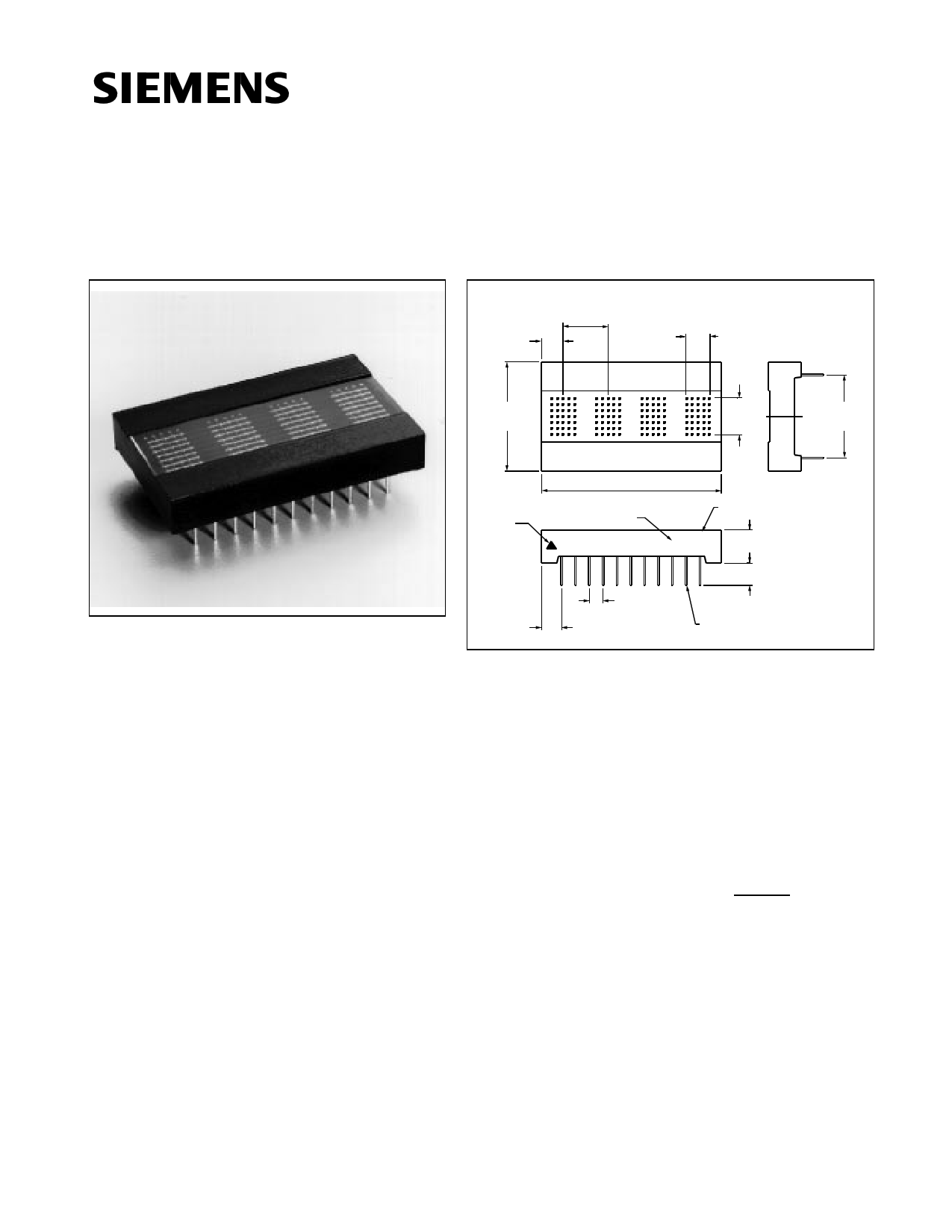
0.270” 4-Character, 5x7 Dot Matrix
Serial Input Dot Addressable Intelligent Display™
Package Dimensions in Inches (mm)
.157 –.007
(3.99 –.18)
.325
(8.26)
.175
(4.45)
.790 –.010
(20.07 –.25)
.270
(6.86)
.600 –.020
(15.25 –.51)
FEATURES
• Four 0.270” (6.85 mm) 5 x 7 Dot Matrix Characters
in Red, High Efficiency Red, High Efficiency Green
• Optimum Display Surface Efficiency (display area
to package ratio)
• High Speed Data Input Rate: 5 MHz
• ROMless Serial Input, Dot Addressable Display
Ideal for User Defined Characters
• Built-in Decoders, Multiplexers and LED Drivers
• Readable from 6 Feet (1.8 meters)
• Wide Viewing Angle, X Axis ±55°, Y Axis ±55°
• Attributes
– 140 Bit RAM for User Defined Characters
– Eight Dimming Levels
– Power Down Model (<250 µW)
– Hardware/Software Clear Functions
– Internal or External Clock
Pin 1
Indicator
1.300 max.
(33.02)
EIA Date Code
Luminous Intensity Code
SCF574X
SIEMENS
Z .276 max.
YYWW (7.0) max.
.100 –.015
(2.54 –.38)
.145 –.015
(3.68 –.38)
.160 –.020
(4.06) –.51)
.018 X .012
(.46 X .30)
(Leads 22 plcs.)
DESCRIPTION
The SCF574X is a four digit, dot addressable 5x7 dot matrix,
serial input, alphanumeric Intelligent Display. The four digits are
packaged in a rugged, high quality, optically transparent, plastic
22 pin DIP with 0.1” pin spacing.
The on-board CMOS has a 140 bit RAM, one bit associated with
one LED, each to generate User Defined Characters. In Power
Down Mode, quiescent current is <50 µA.
The SCF574X is designed for work with the serial port of most
common microprocessors. Data is transferred into the display
through the Serial Data Input (DATA), clocked by the Serial Data
Clock (SDCLK), and enabled by the Load Input (LOAD).
The Clock I/O (CLK I/O) and Clock Select (CLK SEL) pins offer
the user the capability to supply a high speed external multiplex
clock. This feature can minimize audio in-band interference for
portable communication equipment or eliminate the visual
sychronization effects found in high vibration environments such
as avionic equipment.
2–200
1 page 
Top View
22
Pins
12
Digit 0 Digit 1 Digit 2 Digit 3
1 Pins
Pin Assignment
11
Pin Function
Pin Function
1 N/C
2 GND
3 N/C
4 N/C
5 N/C
6 N/C
7 N/C
8 N/C
9 VLL
10 VCC
11 N/C
22 N/C
21 CLKSEL
20 CLK I/O
19 RST
18 N/C
17 N/C
16 N/C
15 SCLK
14 DATA
13 LOAD
12 N/C
0.043
(1.09)
typ.
0.175
(4.45
C1 C2 C3 C4 C5
R0
R1
R2
R3
0.270
(6.86)
R4
0.009
(0.23)
typ.
R5
R6
0.045
(1.14) typ.
Dimensions in inches (mm)
Tolerance: .XXX ± .010 (.25)
Figure 5. Dot Matrix Format
Pin Definitions
Pin Function Definitions
1 N/C
2 GND
Power supply ground
3 N/C
4 N/C
5 N/C
6 N/C
7 N/C
8 N/C
9 VLL
10 VCC
11 N/C
LED supply
Logic supply
12 N/C
13 LOAD
Low input enables data clocking into 8-
bit serial shift register. When load goes
high, the contents of 8-bit serial shift
register will be decoded.
14 DATA
Serial data input
15 SDCLK For loading data into the 8-bit serial
data register
16 N/C
17 N/C
18 N/C
19 RST
Asynchronous input, when low clears
the multiplex counter, address register,
control word register, user RAM and
data registe. Control word register is
set to 100% brightness. The display will
be blank.
20 CLK I/O Outputs Master Clock or inputs Exter-
nal Clock
21 CLKSEL High=Internal Clock (Master)
Low=External Clock (Slave)
22 N/C
2–204
SCF5740/2/4
5 Page 
VCC
40 P3.0 10
18 XTAL2
P3.1
P3.6
11
16
P0.0 39
19 XTAL1
U1
VCC 8031
1 RST
9 P1.0
20
VCC
15 SDCLK GND
13 LD
DATA
ID
19 RST
VCC 10
CLKSEL 21
2 GND CLK I/O 8
14 22 µF
TAN
+
.01 µF
Figure 11. Display Interface to Siemens/Intel 8031 Microprocessor (using one bit of parallel port as serial port)
VCC
VCC
38 40
OSC1
PA0 11
PA1 10
SCLK 33
MOSI 32
39 OSC2
VCC
U1
68HC05C4
1 RST
9 PA2
20
15 SDCLK GND
13 LD
DATA
ID
19 RST
VCC 10
CS 21
2 GND CLK I/O 8
14 22 µF
+TAN
.01 µF
Figure 12. Display Interface with Motoroal 68HC05C4 Microprocessor (using SPI Port)
RST
VCC
RST CLK I/O
CLK SEL
Intelligent Display
DATA SDCLK
LOAD
14 more displays
in between
RST CLK I/O
CLK SEL
Intelligent Display
DATA SDCLK
LOAD
DATA
SDCLK
A0
A1
A2
A3
LD
Chip
0
Address
Decoder 15
CE
Address Decode 1–14
Figure 13. Cascading Multiple Displays
Multiple displays can be cascaded using the CLK SEL and CLK I/O pins (Figure 13). The display designated as the Master-
Clock source should have its CLK SEL pin tied high and the slaves should have their CLK SEL pins tied low. All CLK I/O pins
should be tied together. One display CLK I/O can drive 15 slave CLK I/Os. Use RST to synchronize all display counters.
2–210
SCF5740/2/4
11 Page | ||
| Páginas | Total 12 Páginas | |
| PDF Descargar | [ Datasheet SCF5742.PDF ] | |
Hoja de datos destacado
| Número de pieza | Descripción | Fabricantes |
| SCF5740 | (SCF5740 - SCF5744) Dot Addressable Intelligent Display | Siemens Semiconductor |
| SCF5742 | Dot Matrix Serial Input Dot Addressable Intelligent Display | Siemens |
| SCF5742 | Dot Matrix Serial Input Dot Addressable Intelligent Display | Infineon |
| SCF5742 | (SCF5740 - SCF5744) Dot Addressable Intelligent Display | Siemens Semiconductor |
| Número de pieza | Descripción | Fabricantes |
| SLA6805M | High Voltage 3 phase Motor Driver IC. |
Sanken |
| SDC1742 | 12- and 14-Bit Hybrid Synchro / Resolver-to-Digital Converters. |
Analog Devices |
|
DataSheet.es es una pagina web que funciona como un repositorio de manuales o hoja de datos de muchos de los productos más populares, |
| DataSheet.es | 2020 | Privacy Policy | Contacto | Buscar |