|
|
PDF 3D3523 Data sheet ( Hoja de datos )
| Número de pieza | 3D3523 | |
| Descripción | MONOLITHIC MANCHESTER ENCODER/DECODER | |
| Fabricantes | Data Delay Devices | |
| Logotipo |  |
|
Hay una vista previa y un enlace de descarga de 3D3523 (archivo pdf) en la parte inferior de esta página. Total 5 Páginas | ||
|
No Preview Available !
www.DataSheet4U.com
MONOLITHIC MANCHESTER
ENCODER/DECODER
(SERIES 3D3523)
FEATURES
• All-silicon, low-power CMOS technology
• Encoder and decoder function independently
• Encoder has buffered clock output
• 3.3V operation
• Vapor phase, IR and wave solderable
• Auto-insertable (DIP pkg.)
• Low ground bounce noise
• Maximum data rate: 50 MBaud
• Data rate range: ±15%
• Lock-in time: 1 bit
For mechanical dimensions, click here.
For package marking details, click here.
3D3523
ddealtaay 3
devices, inc.
PACKAGES
CIN 1 14 VDD
CEN 2 13 CBUF
RX 3 12 LOOP
COUT 4 11 TXENB
DIN 5 10 DOUTB
RESB 6
9 TXB
GND 7
8 TX
3D3523-xxx DIP (.300)
3D3523G-xxx Gull Wing (.300)
3D3523D-xxx SOIC (.150)
FUNCTIONAL DESCRIPTION
PIN DESCRIPTIONS
The 3D3523 is a monolithic CMOS Manchester Encoder/Decoder combo
chip. The device uses bi-phase-level encoding to embed a clock signal
into a data stream for transmission across a communications link. In this
encoding mode, a logic one is represented by a high-to-low transition in
the center of the bit cell, while a logic zero is represented by a low-to-high
transition.
The Manchester encoder combines the clock (CIN) and data (DIN) into a
single bi-phase-level signal (TX). An inverted version of this signal (TXB) is
also available. The data baud rate (in MBaud) is equal to the input clock
frequency (in MHz). A replica of the clock input is also available (CBUF).
The encoder may be reset by setting the RESB input low; otherwise, it
should be left high. The TX and TXB signals may be disabled (high-Z) by
setting TXENB high. Similarly, CBUF may be disabled by setting CEN low.
Under most operating conditions, TX and TXB are always enabled, and
CBUF is not used. With this in mind, the 3D3523 provides internal pull-
down resistors on CEN and TXENB, so that most users can leave these
inputs uncommitted.
Encoder:
CIN Clock Input
DIN Data Input
RESB Reset
CEN Clock buffer enable
TXENB Transmit enable
CBUF Buffered clock
TX,TXB Transmitted signal
Decoder:
RX Received Signal
COUT Recovered Clock
DOUTB Recovered Data
Common:
LOOP Loop enable
VDD +3.3 Volts
GND Ground
The Manchester decoder accepts the embedded-clock signal at the RX input. The recovered clock and
data signals are presented on COUT and DOUTB, respectively, with the data signal inverted. The
operating baud rate (in MBaud) is specified by the dash number of the device. The input baud rate may
vary by as much as ±15% from the nominal device baud rate without compromising the integrity of the
information received.
Because the decoder is not PLL-based, it does not require a long preamble in order to lock onto the
received signal. Rather, the device requires at most one bit cell before the data presented at the output is
valid. This is extremely useful in cases where the information arrives in bursts and the input is otherwise
turned off.
Normally, the encoder and decoder function independently. However, if the LOOP input is set high, the
encoded TX signal is fed back internally into the decoder and the RX input is ignored. This feature is
useful for diagnostics. The LOOP input has an internal pull-down resistor and may be left uncommitted if
this feature is not needed.
2006 Data Delay Devices
Doc #06006
5/8/2006
DATA DELAY DEVICES, INC.
3 Mt. Prospect Ave. Clifton, NJ 07013
1
1 page 
3D3523
AUTOMATED TESTING - MONOLITHIC PRODUCTS
TEST CONDITIONS
INPUT:
Ambient Temperature: 25oC ± 3oC
Supply Voltage (Vcc): 5.0V ± 0.1V
Input Pulse:
High = 3.0V ± 0.1V
Low = 0.0V ± 0.1V
Source Impedance: 50Ω Max.
Rise/Fall Time:
3.0 ns Max. (measured
between 0.6V and 2.4V )
Pulse Width:
Period:
PWIN = 1/(2*BAUD)
PERIN = 1/BAUD
OUTPUT:
Rload:
Cload:
Threshold:
10KΩ ± 10%
5pf ± 10%
1.5V (Rising & Falling)
Device
Under
Test
10KΩ
470Ω
Digital
Scope
5pf
NOTE: The above conditions are for test only and do not in any way restrict the operation of the device.
COMPUTER
SYSTEM
PRINTER
W AVEFORM
GENERATOR
OUT
TRIG
IN DEVICE UNDER OUT IN
TEST (DUT)
TRIG
DIGITAL SCOPE
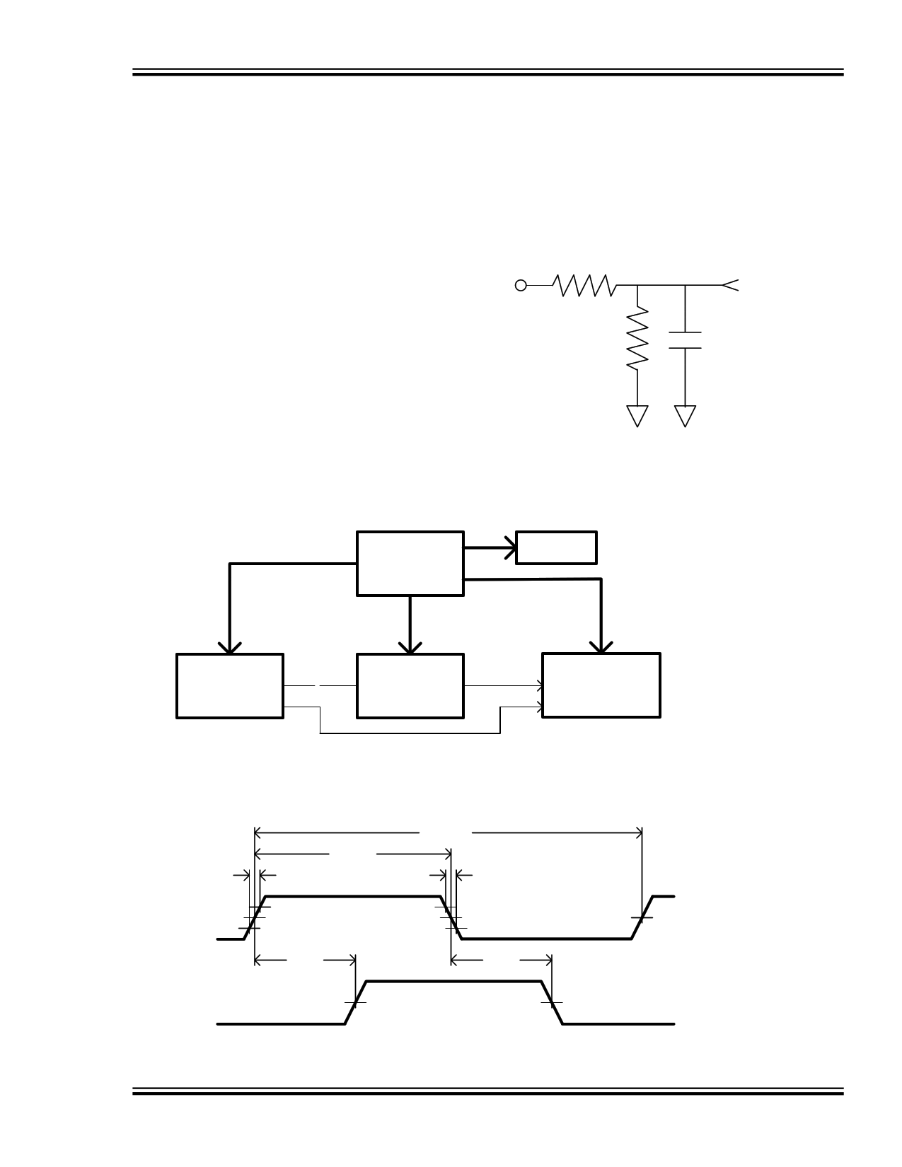
Figure 3: Test Setup
INPUT
SIGNAL
OUTPUT
SIGNAL
tRISE
2.4V
1.5V
0.6V
tPLH
PWIN
PERIN
tFALL
VIH 2.4V
1.5V
0.6V
VIL
tPHL
1.5V
VOH
1.5V
Figure 4: Timing Diagram
VOL
Doc #06006
5/8/2006
DATA DELAY DEVICES, INC.
3 Mt. Prospect Ave. Clifton, NJ 07013
5
5 Page | ||
| Páginas | Total 5 Páginas | |
| PDF Descargar | [ Datasheet 3D3523.PDF ] | |
Hoja de datos destacado
| Número de pieza | Descripción | Fabricantes |
| 3D3521 | MONOLITHIC MANCHESTER ENCODER | Data Delay Devices |
| 3D3522 | MONOLITHIC MANCHESTER ENCODER | Data Delay Devices |
| 3D3523 | MONOLITHIC MANCHESTER ENCODER/DECODER | Data Delay Devices |
| Número de pieza | Descripción | Fabricantes |
| SLA6805M | High Voltage 3 phase Motor Driver IC. |
Sanken |
| SDC1742 | 12- and 14-Bit Hybrid Synchro / Resolver-to-Digital Converters. |
Analog Devices |
|
DataSheet.es es una pagina web que funciona como un repositorio de manuales o hoja de datos de muchos de los productos más populares, |
| DataSheet.es | 2020 | Privacy Policy | Contacto | Buscar |
