|
|
|
PDF NL7SZ18 Data sheet ( Hoja de datos )
| Número de pieza | NL7SZ18 | |
| Descripción | 1-of-2 Non-Inverting Demultiplexer | |
| Fabricantes | ON Semiconductor | |
| Logotipo | ||
Hay una vista previa y un enlace de descarga de NL7SZ18 (archivo pdf) en la parte inferior de esta página. Total 7 Páginas | ||
|
No Preview Available !
www.DataSheet4U.com
NL7SZ18
1−of−2 Non−Inverting
Demultiplexer with 3−State
Deselected Output
The NL7SZ18 is a high−performance 1−to−2 Demultiplexer
operating from a 1.65 V to 5.5 V supply. When the select pin [S] is
enabled [high or low], the data in the address pin [A] is routed to one of
the output pins [Y0 or Y1], maintaining a high−impedance on the
deselected output pin (See Truth Table).
This device has been optimized for on−board buffering applications
and offers mixed (1.65 V, 2.3 V, 3.0 V and 5.5 V) voltage capability by
providing over voltage tolerance (OVT*) circuitry on I/O pins.
Features
• High−Speed Propagation Delay
tPD 2.5 nS (Typ), Load 50 pF @ 5.0 V
• Power Down Impedance
Outputs in High−Z
• Output Drive Capability
32 mA @ 5.0 V
• Broad VCC Operating Range
1.65 V to 5.5 V
• Surface Mount Technology
SC−70, 6−Lead Packaging
• OVT* on Inputs/Outputs
• Pb−Free Package is Available
Typical Applications
• Cell Phones
• PDAs
• Digital Cameras
• Video Cameras
Important Information
• ESD Protection: MM >200 V, Human Body Model >2000 V
• Latch−Up Max Rating: 300 mA
• Pin−to−Pin Compatible with NC7SZ18
*Over Voltage Tolerance (OVT) enables input and output pins to function outside
(higher) of their operating voltages, with no damage to the devices or to signal
integrity.
PIN/FUNCTION TABLE
Pin Function
A Data Input
S Demultiplexer Select
Y0 Output 1
Y1 Output 2
© Semiconductor Components Industries, LLC, 2006
November, 2006 − Rev. 6
1
http://onsemi.com
MARKING DIAGRAMS
1
SOT−363/SC70−6/SC−88
DF SUFFIX
CASE 419B
1
LD M G
G
1
UDFN6
MU SUFFIX
CASE 517AA
TM
G
LD, T
M
G
= Device Marking
= Date Code*
= Pb−Free Package
(Note: Microdot may be in either location)
*Date Code orientation and/or position may vary
depending upon manufacturing location.
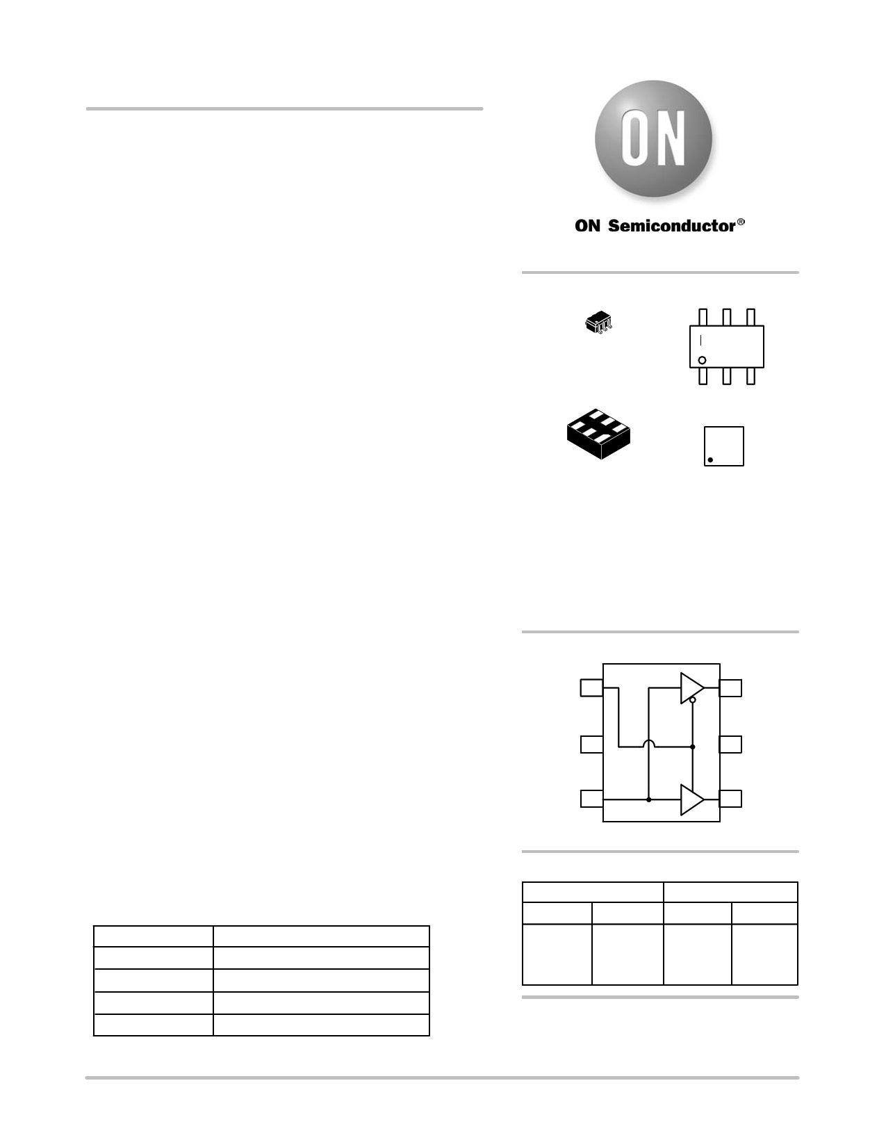
PIN ASSIGNMENT
S1
6 Y0
GND 2
5 VCC
A3
4 Y1
(TOP VIEW)
TRUTH TABLE
Input
Output
S A Y0 Y1
L LLZ
L HHZ
H LZL
H HZH
ORDERING INFORMATION
See detailed ordering and shipping information in the package
dimensions section on page 2 of this data sheet.
Publication Order Number:
NL7SZ18/D
1 page 
tr = 3 nS
A Input
10%
tPLH
NL7SZ18
90%
50%
90%
50%
tf = 3 nS
VCC
10%
GND
tPHL
VOH
Output
50%
50%
VOL
90%
IR = tF = 3 nS
90%
S Input
50%
50%
10%
tPZL
10%
tPLZ
Output
50%
Output
tPZH
50%
tPHZ
VOL + 0.3 V
VOH − 0.3 V
VCC
GND
VOL
VOH
Figure 3. AC Waveforms
http://onsemi.com
5
5 Page | ||
| Páginas | Total 7 Páginas | |
| PDF Descargar | [ Datasheet NL7SZ18.PDF ] | |
Hoja de datos destacado
| Número de pieza | Descripción | Fabricantes |
| NL7SZ18 | 1-of-2 Non-Inverting Demultiplexer | ON Semiconductor |
| NL7SZ19 | 1-of-2 Decoder/ Demultiplexer | ON Semiconductor |
| Número de pieza | Descripción | Fabricantes |
| SLA6805M | High Voltage 3 phase Motor Driver IC. |
Sanken |
| SDC1742 | 12- and 14-Bit Hybrid Synchro / Resolver-to-Digital Converters. |
Analog Devices |
|
DataSheet.es es una pagina web que funciona como un repositorio de manuales o hoja de datos de muchos de los productos más populares, |
| DataSheet.es | 2020 | Privacy Policy | Contacto | Buscar |