|
|
|
PDF NID9N05CL Data sheet ( Hoja de datos )
| Número de pieza | NID9N05CL | |
| Descripción | Power MOSFET ( Transistor ) | |
| Fabricantes | ON Semiconductor | |
| Logotipo | ||
Hay una vista previa y un enlace de descarga de NID9N05CL (archivo pdf) en la parte inferior de esta página. Total 8 Páginas | ||
|
No Preview Available !
www.DataSheet4U.com
NID9N05CL
Power MOSFET
9.0 A, 52 V, N−Channel, Logic Level,
Clamped MOSFET w/ ESD Protection
in a DPAK Package
Benefits
• High Energy Capability for Inductive Loads
• Low Switching Noise Generation
Features
• Diode Clamp Between Gate and Source
• ESD Protection − HBM 5000 V
• Active Over−Voltage Gate to Drain Clamp
• Scalable to Lower or Higher RDS(on)
• Internal Series Gate Resistance
Applications
• Automotive and Industrial Markets:
Solenoid Drivers, Lamp Drivers, Small Motor Drivers
MAXIMUM RATINGS (TJ = 25°C unless otherwise noted)
Rating
Symbol Value
Unit
Drain−to−Source Voltage Internally Clamped
Gate−to−Source Voltage − Continuous
Drain Current − Continuous @ TA = 25°C
Drain Current − Single Pulse (tp = 10 ms)
Total Power Dissipation @ TA = 25°C
Operating and Storage Temperature Range
VDSS
VGS
ID
IDM
PD
TJ, Tstg
52−59
±15
9.0
35
28.8
−55 to
175
V
V
A
W
°C
Single Pulse Drain−to−Source Avalanche
Energy − Starting TJ = 125°C
(VDD = 50 V, ID(pk) = 1.5 A, VGS = 10 V,
RG = 25 W)
Thermal Resistance − Junction−to−Case
− Junction−to−Ambient (Note 1)
− Junction−to−Ambient (Note 2)
Maximum Lead Temperature for Soldering
Purposes, 1/8″ from Case for 10 s
EAS 160 mJ
RqJC
RqJA
RqJA
TL
5.2 °C/W
72
100
260 °C
Maximum ratings are those values beyond which device damage can occur.
Maximum ratings applied to the device are individual stress limit values (not
normal operating conditions) and are not valid simultaneously. If these limits are
exceeded, device functional operation is not implied, damage may occur and
reliability may be affected.
1. When surface mounted to an FR4 board using 1″ pad size, (Cu area 1.127 in2)
2. When surface mounted to an FR4 board using minimum recommended pad
size, (Cu area 0.412 in2)
http://onsemi.com
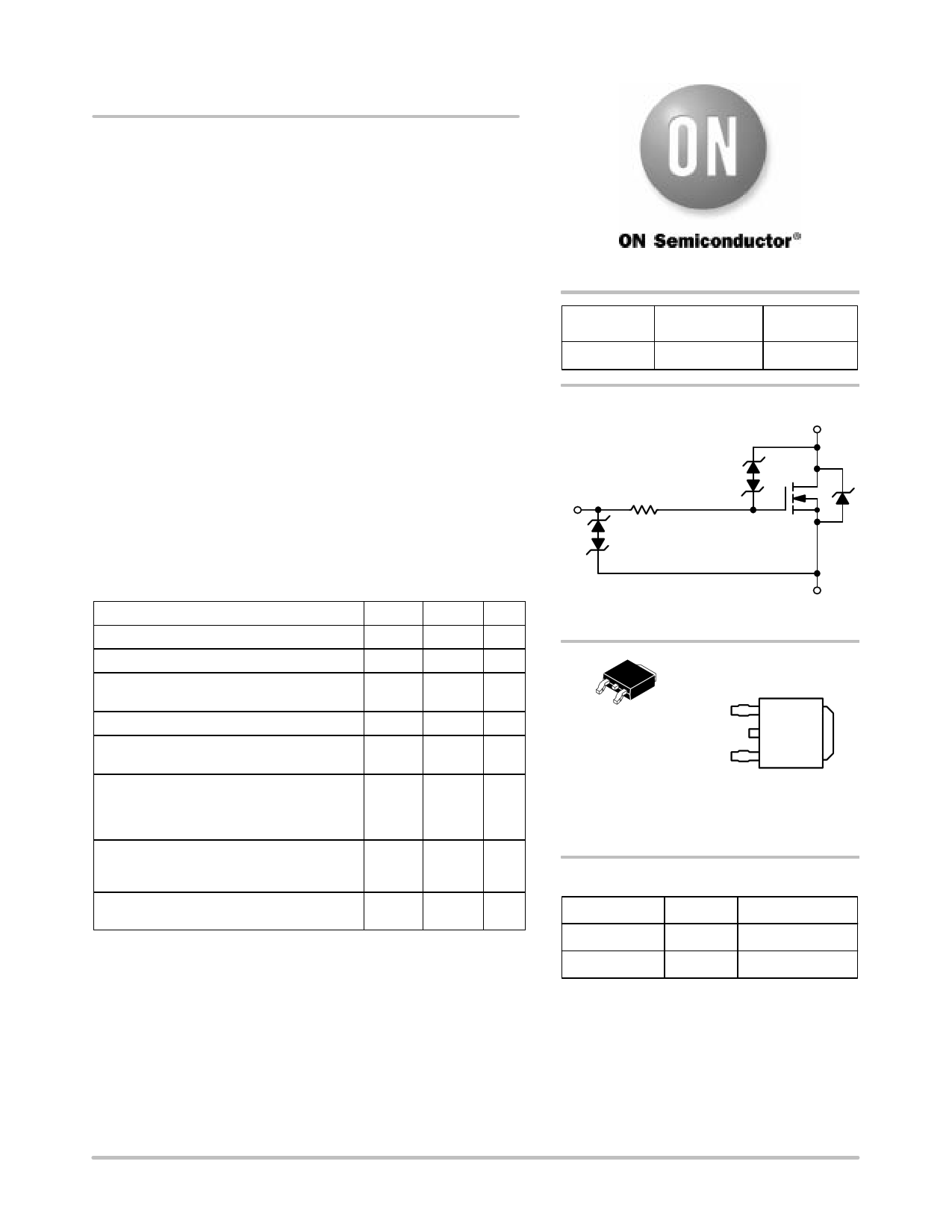
VDSS
(Clamped)
52 V
RDS(ON) TYP
90 mΩ
ID MAX
(Limited)
9.0 A
Drain
(Pins 2, 4)
Gate
(Pin 1)
Overvoltage
Protection
RG
ESD Protection
MPWR
Source
(Pin 3)
MARKING
DIAGRAM
DPAK
CASE 369C
STYLE 2
1
2
3
AYWW
D9N05CL
4
D9N05CL
A
Y
WW
= Device Code
= Assembly Location
= Year
= Work Week
1 = Gate
2 = Drain
3 = Source
4 = Drain
ORDERING INFORMATION
Device
Package
Shipping†
NID9N05CLT4
NID9N05CL
DPAK
DPAK
2500/Tape & Reel
75 Units/Rail
†For information on tape and reel specifications,
including part orientation and tape sizes, please
refer to our Tape and Reel Packaging Specification
Brochure, BRD8011/D.
© Semiconductor Components Industries, LLC, 2004
July, 2004 − Rev. 5
1
Publication Order Number:
NID9N05CL/D
1 page 
NID9N05CL
500
Frequency = 10 kHz
TJ = 25°C
400 VGS = 0 V
300
200 Ciss
100 Coss
Crss
0
0 10 20 30 40
VDS, DRAIN−TO−SOURCE VOLTAGE (VOLTS)
Figure 7. Capacitance Variation
50
5
4
Qgs
3
50
QT
VGS
40
Qgd
30
2
VDS
1
ID = 9 A
TJ = 25°C
20
10
00
01 2 3 45
Qg, TOTAL GATE CHARGE (nC)
Figure 8. Gate−To−Source and Drain−To−Source
Voltage versus Total Charge
10,000
VDD = 40 V
ID = 9 A
VGS = 10 V
1000
td(off)
tf
tr
100
1
td(on)
10
RG, GATE RESISTANCE (OHMS)
Figure 9. Resistive Switching Time
Variation versus Gate Resistance
DRAIN−TO−SOURCE DIODE CHARACTERISTICS
10
VGS = 0 V
TJ = 25°C
8
100
6
4
2
0
0.4 0.6 0.8 1.0
VSD, SOURCE−TO−DRAIN VOLTAGE (VOLTS)
1.2
Figure 10. Diode Forward Voltage versus Current
http://onsemi.com
5
5 Page | ||
| Páginas | Total 8 Páginas | |
| PDF Descargar | [ Datasheet NID9N05CL.PDF ] | |
Hoja de datos destacado
| Número de pieza | Descripción | Fabricantes |
| NID9N05CL | Power MOSFET ( Transistor ) | ON Semiconductor |
| Número de pieza | Descripción | Fabricantes |
| SLA6805M | High Voltage 3 phase Motor Driver IC. |
Sanken |
| SDC1742 | 12- and 14-Bit Hybrid Synchro / Resolver-to-Digital Converters. |
Analog Devices |
|
DataSheet.es es una pagina web que funciona como un repositorio de manuales o hoja de datos de muchos de los productos más populares, |
| DataSheet.es | 2020 | Privacy Policy | Contacto | Buscar |