|
|
|
PDF NCP9002 Data sheet ( Hoja de datos )
| Número de pieza | NCP9002 | |
| Descripción | Audio Power Amplifier | |
| Fabricantes | ON Semiconductor | |
| Logotipo | ||
Hay una vista previa y un enlace de descarga de NCP9002 (archivo pdf) en la parte inferior de esta página. Total 13 Páginas | ||
|
No Preview Available !
www.DataSheet4U.com
NCP9002
1.3 Watt Audio Power
Amplifier with Fast Turn On
Time
The NCP9002 is an audio power amplifier designed for portable
communication device applications such as mobile phone
applications. The NCP9002 is capable of delivering 1.3 W of
continuous average power to an 8.0 W BTL load from a 5.0 V power
supply, and 1.0 W to a 4.0 W BTL load from a 3.6 V power supply.
The NCP9002 provides high quality audio while requiring few
external components and minimal power consumption. It features a
low−power consumption shutdown mode, which is achieved by
driving the SHUTDOWN pin with logic low.
The NCP9002 contains circuitry to prevent from “pop and click”
noise that would otherwise occur during turn−on and turn−off
transitions.
For maximum flexibility, the NCP9002 provides an externally
controlled gain (with resistors), as well as an externally controlled
turn−on time (with the bypass capacitor). When using a 1 mF bypass
capacitor, it offers 100 ms wake up time.
Due to its excellent PSRR, it can be directly connected to the
battery, saving the use of an LDO.
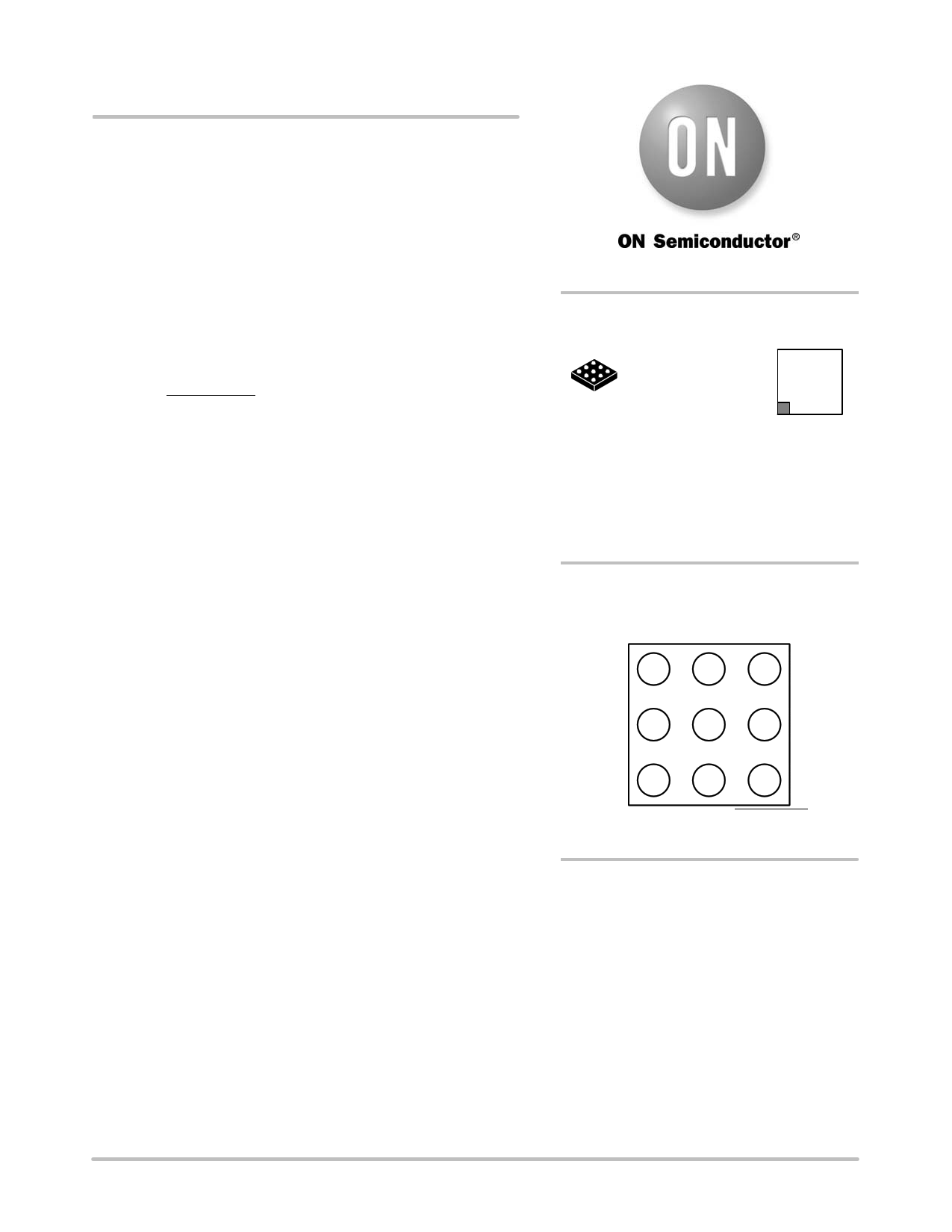
This device is available in a 9−Pin Flip−Chip CSP (Lead−Free).
Features
• 1.3 W to an 8.0 W BTL Load from a 5.0 V Power Supply
• Excellent PSRR: Direct Connection to the Battery
• “Pop and Click” Noise Protection Circuit
• Ultra Low Current Shutdown Mode: 10 nA
• 2.2 V−5.5 V Operation
• External Gain Configuration Capability
• External Turn−on Time Configuration Capability:
100 ms (1 mF Bypass Capacitor)
• Up to 1.0 nF Capacitive Load Driving Capability
• Thermal Overload Protection Circuitry
• This is a Pb−Free Device
Typical Applications
• Portable Electronic Devices
• PDAs
• Wireless Phones
http://onsemi.com
MARKING
DIAGRAMS
9−Pin Flip−Chip CSP A3
FC SUFFIX
MAZG
A1 CASE 499AL
AYWW
C1
A1
MAZ
A
Y
WW
G
= Specific Device Code
= Assembly Location
= Year
= Work Week
= Pb−Free Package
PIN CONNECTIONS
9−Pin Flip−Chip CSP
A1 A2
INM OUTA
B1
VM_P
C1
B2
VM
C2
A3
INP
B3
Vp
C3
BYPASS OUTB SHUTDOWN
(Top View)
ORDERING INFORMATION
See detailed ordering and shipping information in the package
dimensions section on page 12 of this data sheet.
© Semiconductor Components Industries, LLC, 2006
December, 2006 − Rev. 4
1
Publication Order Number:
NCP9002/D
1 page 
NCP9002
TYPICAL PERFORMANCE CHARACTERISTICS
10
Vp = 2.5 V
RL = 8 W
1 f = 1 kHz
AV = 2
0.1
10
Vp = 3.2 V
1
RL = 8 W
f = 1 kHz
AV = 2
0.1
0.01 0.01
0.001
0
0.001
50 100 150 200 250 300 350 400
0
Pout, POWER OUT (mW)
Figure 3. THD + N versus Power Out
100 200 300 400 500 600
Pout, POWER OUT (mW)
Figure 4. THD + N versus Power Out
700
10
Vp = 3.6 V
1
RL = 8 W
f = 1 kHz
AV = 2
0.1
10
Vp = 4.2 V
1
RL = 8 W
f = 1 kHz
AV = 2
0.1
0.01 0.01
0.001
0
100 200 300 400 500 600 700
Pout, POWER OUT (mW)
Figure 5. THD + N versus Power Out
800
0.001
0
200 400 600 800 1000
Pout, POWER OUT (mW)
Figure 6. THD + N versus Power Out
1200
10
Vp = 5 V
1 RL = 8 W
f = 1 kHz
AV = 2
0.1
10
Vp = 3.6 V
1
RL = 4 W
f = 1 kHz
AV = 2
0.1
0.01 0.01
0.001
0
200 400 600 800 1000 1200 1400 1600
Pout, POWER OUT (mW)
Figure 7. THD + N versus Power Out
0.001
0
200 400 600 800 1000
Pout, POWER OUT (mW)
Figure 8. THD + N versus Power Out
1200
http://onsemi.com
5
5 Page 
NCP9002
APPLICATION INFORMATION
Detailed Description
The NCP9002 audio amplifier can operate under 2.6 V
until 5.5 V power supply. With less than 1% THD+N, B
version can deliver up to 1.2 W rms output power to an
8.0 W load (Vp = 5.0 V). If application allows to reach 10%
THD+N, then 1.6 W can be provided using a 5.0 V power
supply.
The structure of the NCP9002 is basically composed of
two identical internal power amplifiers; the first one is
externally configurable with gain−setting resistors Rin and
Rf (the closed−loop gain is fixed by the ratios of these
resistors) and the second is internally fixed in an inverting
unity−gain configuration by two resistors of 20 kW. So the
load is driven differentially through OUTA and OUTB
outputs. This configuration eliminates the need for an
output coupling capacitor. The NCP9002 has around 10 kW
output impedance in the shutdown mode.
Internal Power Amplifier
The output PMOS and NMOS transistors of the amplifier
were designed to deliver the output power of the
specifications without clipping. The channel resistance
(Ron) of the NMOS and PMOS transistors does not exceed
0.6 W when they drive current.
The structure of the internal power amplifier is
composed of three symmetrical gain stages, first and
medium gain stages are transconductance gain stages to
obtain maximum bandwidth and DC gain.
Turn−On and Turn−Off Transitions
A cycle with a turn−on and turn−off transition is
illustrated with plots that show both single ended signals on
the previous page.
In order to eliminate “pop and click” noises during
transitions, output power in the load must be slowly
established or cut. When logic high is applied to the
shutdown pin, the bypass voltage begins to rise
exponentially and once the output DC level is around the
common mode voltage, the gain is established
instantaneously. This way to turn−on the device is
optimized in terms of rejection of “pop and click” noises.
The device has the same behavior when it is turned−off
by a logic low on the shutdown pin. During the shutdown
mode, amplifier outputs are connected to the ground.
When a shutdown low level is applied, with 1 mF bypass
capacitor, it takes 65 ms before the DC output level is tied
to Ground on each output. However, no audio signal will be
provided to the BTL load only 1 ms after the falling edge on
the shutdown pin.
With 1 mF bypass capacitor, turn on time is set to 90 ms.
This fast turn on time added to a very low shutdown current
saves battery life and brings flexibility when designing the
audio section of the final application.
NCP9002 is a zero pop noise device when using a
differential audio input. In case of a single ended one, there
is no audible pop click noise, especially when the input cut
off frequency is higher than 100 Hz.
Shutdown Function
The device enters shutdown mode when shutdown signal
is low. During the shutdown mode, the DC quiescent
current of the circuit does not exceed 100 nA. In this
configuration, the output impedance is 10 kW on each
output.
Current Limit Circuit
The maximum output power of the circuit (Porms =
1.0 W, Vp = 5.0 V, RL = 8.0 W) requires a peak current in
the load of 500 mA.
In order to limit the excessive power dissipation in the
load when a short−circuit occurs, the current limit in the
load is fixed to 800 mA. The current in the four output MOS
transistors are real−time controlled, and when one current
exceeds 800 mA, the gate voltage of the MOS transistor is
clipped and no more current can be delivered.
Thermal Overload Protection
Internal amplifiers are switched off when the
temperature exceeds 160°C, and will be switched on again
only when the temperature decreases fewer than 140°C.
The NCP9002 is unity−gain stable and requires no
external components besides gain−setting resistors, an
input coupling capacitor and a proper bypassing capacitor
in the typical application.
The first amplifier is externally configurable (Rf and
Rin), while the second is fixed in an inverting unity gain
configuration.
The differential−ended amplifier presents two major
advantages:
− The possible output power is four times larger (the
output swing is doubled) as compared to a single−ended
amplifier under the same conditions.
− Output pins (OUTA and OUTB) are biased at the same
potential Vp/2, this eliminates the need for an output
coupling capacitor required with a single−ended
amplifier configuration.
The differential closed loop−gain of the amplifier is
given
by
Avd
+
2
*
Rf
Rin
+
Vorms
Vinrms
.
Output power delivered to the load is given by
Porms
+
(Vopeak)2
2 * RL
(Vopeak
is
the
peak
differential
output voltage).
When choosing gain configuration to obtain the desired
output power, check that the amplifier is not current limited
or clipped.
The maximum current which can be delivered to the load
is
500
mA
Iopeak
+
Vopeak
RL
.
http://onsemi.com
11
11 Page | ||
| Páginas | Total 13 Páginas | |
| PDF Descargar | [ Datasheet NCP9002.PDF ] | |
Hoja de datos destacado
| Número de pieza | Descripción | Fabricantes |
| NCP9001 | Adjustable Output Voltage Step-Down Converter | ON Semiconductor |
| NCP9002 | Audio Power Amplifier | ON Semiconductor |
| NCP9003 | Compact Backlight LED Boost Driver | ON Semiconductor |
| NCP9004 | Filterless Class-D Audio Power Amplifier | ON Semiconductor |
| Número de pieza | Descripción | Fabricantes |
| SLA6805M | High Voltage 3 phase Motor Driver IC. |
Sanken |
| SDC1742 | 12- and 14-Bit Hybrid Synchro / Resolver-to-Digital Converters. |
Analog Devices |
|
DataSheet.es es una pagina web que funciona como un repositorio de manuales o hoja de datos de muchos de los productos más populares, |
| DataSheet.es | 2020 | Privacy Policy | Contacto | Buscar |