|
|
|
PDF NCP4894 Data sheet ( Hoja de datos )
| Número de pieza | NCP4894 | |
| Descripción | Differential Audio Power Amplifier | |
| Fabricantes | ON Semiconductor | |
| Logotipo | ||
Hay una vista previa y un enlace de descarga de NCP4894 (archivo pdf) en la parte inferior de esta página. Total 18 Páginas | ||
|
No Preview Available !
www.DataSheet4U.com
NCP4894
1.8 Watt Differential Audio
Power Amplifier with
Selectable Shutdown
The NCP4894 is a differential audio power amplifier designed for
portable communication device applications. This feature and the
excellent audio characteristics of the NCP4894 are a guarantee of a
high quality sound, for example, in mobile phones applications. With
a 10% THD+N value the NCP4894 is capable of delivering 1.8 W of
continuous average power to an 8.0 W load from a 5.5 V power
supply. With the same load conditions and a 5.0 V battery voltage, it
ensures 1.0 W to be delivered with less than 0.01% distortion.
The NCP4894 provides high quality audio while requiring few
external components and minimal power consumption. It features a
low−power consumption shutdown mode.
To be flexible, shutdown may be enabled by either a logic high or
low depending on the voltage applied on the SD MODE pin.
The NCP4894 contains circuitry to prevent from “pop and click”
noise that would otherwise occur during turn−on and turn−off
transitions.
For maximum flexibility, the NCP4894 provides an externally
controlled gain (with resistors), as well as an externally controlled
turn−on time (with bypass capacitor).
Due to its excellent PSRR, it can be directly connected to the
battery, saving the use of an LDO.
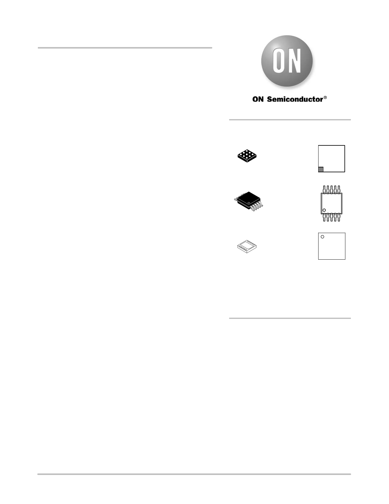
This device is available in 9−Pin Flip−Chip, Micro−10 and DFN10
3x3 mm packages.
Features
• Differential Amplification
• Shutdown High or Low Selectivity
• 1.0 W to an 8.0 W Load from a 5.0 V Power Supply
• Superior PSRR: Direct Connection to the Battery
• “Pop and Click” Noise Protection Circuit
• Ultra Low Current Shutdown Mode
• 2.2 V−5.5 V Operation
• External Gain Configuration Capability
• External Turn−on Configuration Capability
• Thermal Overload Protection Circuitry
• Pb−Free Packages are Available
Typical Applications
• Portable Electronic Devices
• PDAs
• Mobile Phones
http://onsemi.com
MARKING
DIAGRAMS
1
9−PIN FLIP−CHIP
FC SUFFIX
CASE 499AL
A3
xxxG
AYWW
C1
A1
8
1
Micro−10
DM SUFFIX
CASE 846B
xxxx
AYWG
G
DFN10
1
MN SUFFIX
xxx
CASE 485C
ALYWG
1G
xxxx = Specific Device Code
A = Assembly Location
L = Wafer Lot
Y = Year
W, WW = Work Week
G = Pb−Free Package
(Note: Microdot may be in either location)
ORDERING INFORMATION
See detailed ordering and shipping information in the package
dimensions section on page 14 of this data sheet.
© Semiconductor Components Industries, LLC, 2005
November, 2005 − Rev. 8
1
Publication Order Number:
NCP4894/D
1 page 
NCP4894
ELECTRICAL CHARACTERISTICS Limits apply for TA between −40°C to +85°C (Unless otherwise noted).
Characteristic
Symbol
Conditions
Min
(Note 8)
Typ
Supply Quiescent Current
Idd
VP = 3.0 V, No Load
− 1.9
VP = 5.0 V, No Load
− 2.1
VP = 3.0 V, 8.0 W
VP = 5.0 V, 8.0 W
− 2.0
− 2.2
Common Mode Voltage
Shutdown Current
SD SELECT Threshold High
SD SELECT Threshold Low
Turning On Time (Note 10)
Turning Off Time (Note 10)
Output Swing
Rms Output Power
Vcm
ISD
VSDIH
VSDIL
TWU
TSD
Vloadpeak
PO
−
For VP between 2.2 V to 5.5 V
SDM = SDS = GND
TA = 25°C
TA = −40°C to +85°C
−
−
Cby = 1.0 mF
−
VP = 3.0 V, RL = 8.0 W
VP = 5.0 V, RL = 8.0 W (Note 9)
TA = 25°C
TA = −40°C to +85°C
VP = 3.0 V, RL = 8.0 W
THD + N < 0.1%
VP = 3.3 V, RL = 8.0 W
THD + N < 0.1%
VP = 5.0 V, RL = 8.0 W
THD + N < 0.1%
−
−
−
1.4
−
−
−
−
4.0
3.85
−
−
−
VP/2
20
−
−
−
140
20
2.5
4.3
−
0.39
0.48
1.08
Output Offset Voltage
VOS
For VP between 2.2 V
−30 1.0
to 5.5 V
Power Supply Rejection Ratio
PSRR V+
G = 2.0, RL = 8.0 W
VPripple_pp = 200 mV
Cby = 1.0 mF
Input Terminated with 10 W
Max
(Note 8)
−
−
−
4.0
−
Unit
mA
V
600 nA
2.0 mA
−V
0.4 V
− ms
− ms
−V
V
−
−
−W
−
−
30 mV
dB
F = 217 Hz
VP = 5.0 V
VP = 3.0 V
− −80 −
− −80 −
F = 1.0 kHz
VP = 5.0 V
VP = 3.0 V
− −85 −
− −85 −
Efficiency
Thermal Shutdown Temperature
Total Harmonic Distortion
h
VP = 3.0 V, Porms = 380 mW
−
64
−%
VP = 5.0 V, Porms = 1.0 W
−
63
−
Tsd − 160 − °C
THD
VP = 3.0 V, F = 1.0 kHz
RL = 8.0 W, AV = 2.0
PO = 0.32 W
−−−
− 0.007 −
−−−
%
VP = 5.0 V, F = 1.0 kHz
RL = 8.0 W, AV = 2.0
PO = 1.0 W
−−−
− 0.006 −
−−−
8. Min/Max limits are guaranteed by design, test or statistical analysis.
9. This parameter is not tested in production for 9−Pin Flip−Chip CSP package in case of a 5.0 V power supply, however it is correlated based
on a 3.0 V power supply testing.
10. See page 11 for a theoretical approach of these parameters.
http://onsemi.com
5
5 Page 
NCP4894
APPLICATION INFORMATION
Detailed Description
The NCP4894 audio amplifier can operate under 2.6 V
until 5.5 V power supply. It delivers 320 mW rms output
power to 4.0 W load (VP = 2.6 V) and 1.0 W rms output
power to 8.0 W load (VP = 5.0 V).
The structure of the NCP4894 is basically composed of
two identical internal power amplifiers. Both are externally
configurable with gain−setting resistors Rin and Rf (the
closed−loop gain is fixed by the ratios of these resistors).
The load is driven differentially through OUTA and OUTB
outputs. This configuration eliminates the need for an
output coupling capacitor.
Internal Power Amplifier
The output PMOS and NMOS transistors of the amplifier
were designed to deliver the output power of the
specifications without clipping. The channel resistance
(Ron) of the NMOS and PMOS transistors does not exceed
0.6 W when they drive current.
The structure of the internal power amplifier is
composed of three symmetrical gain stages, first and
medium gain stages are transconductance gain stages to
obtain maximum bandwidth and DC gain.
Turn−On and Turn−Off Transitions
A cycle with a turn−on and turn−off transition is
illustrated with plots that show both single ended signals on
the previous page.
In order to eliminate “pop and click” noises during
transitions, output power in the load must be slowly
established or cut. When logic high is applied to the
shutdown pin, the bypass voltage begins to rise
exponentially and once the output DC level is around the
common mode voltage, the gain is established slowly
(20 ms). Using this turn−on mode, the device is optimized
in terms of rejection of “pop and click” noises.
A theoretical value of turn−on time at 25°C is given by
the following formula.
Cby: bypass capacitor
R: internal 150 k resistor with a 25% accuracy
Ton = 0.95 * R * Cby
The device has the same behavior when it is turned−off
by a logic low on the shutdown pin. During the shutdown
mode, amplifier outputs are connected to the ground.
However, to totally cut the output audio signal, you only
need to wait for 20 ms.
During the shutdown state, the DC quiescent current has a
typical value of 10 nA.
Current Limit Circuit
The maximum output power of the circuit
(Porms = 1.0 W, VP = 5.0 V, RL = 8.0 W) requires a peak
current in the load of 500 mA.
In order to limit the excessive power dissipation in the
load when a short−circuit occurs between both outputs, the
current limit in the load is fixed to 800 mA.
Thermal Overload Protection
Internal amplifiers are switched off when the
temperature exceeds 160°C, and will be switched on again
only when the temperature decreases below 140°C.
The NCP4894 is unity−gain stable and requires no
external components besides gain−setting resistors, an
input coupling capacitor and a proper bypassing capacitor
in the typical application.
Both internal amplifiers are externally configurable (Rf
and Rin) with gain configuration.
The differential−ended amplifier presents two major
advantages:
− The possible output power is four times larger (the
output swing is doubled) as compared to a single−ended
amplifier under the same conditions.
− Output pins (OUTA and OUTB) are biased at the same
potential VP/2, this eliminates the need for an output
coupling capacitor required with a single−ended
amplifier configuration.
The differential closed loop−gain of the amplifier is
given
by
Avd
+
*
Rf
Rin
+
Vorms
Vinrms
. Vorms
is
the
rms
value
of
the voltage seen by the load and Vinrms is the rms value of
the input differential signal.
Output power delivered to the load is given by
Porms
+
(Vopeak)2
2 * RL
(Vopeak
is
the
peak
differential
output voltage).
When choosing gain configuration to obtain the desired
output power, check that the amplifier is not current limited
or clipped.
The maximum current which can be delivered to the load
is
500
mA
Iopeak
+
Vopeak
RL
.
Shutdown Function
The device enters shutdown mode once the SD SELECT
and SD MODE pins are in the same logic state. This brings
flexibility to the design, as the SD MODE pin must be
permanently connected to VP or GND on the PCB. If the
SD SELECT pin is not connected to the output of a
microcontroller or microprocessor, it’s not advisable to let
it float. A pulldown or pullup resistor is then suitable.
http://onsemi.com
11
11 Page | ||
| Páginas | Total 18 Páginas | |
| PDF Descargar | [ Datasheet NCP4894.PDF ] | |
Hoja de datos destacado
| Número de pieza | Descripción | Fabricantes |
| NCP4894 | Differential Audio Power Amplifier | ON Semiconductor |
| NCP4896 | Audio Power Amplifier | ON Semiconductor |
| Número de pieza | Descripción | Fabricantes |
| SLA6805M | High Voltage 3 phase Motor Driver IC. |
Sanken |
| SDC1742 | 12- and 14-Bit Hybrid Synchro / Resolver-to-Digital Converters. |
Analog Devices |
|
DataSheet.es es una pagina web que funciona como un repositorio de manuales o hoja de datos de muchos de los productos más populares, |
| DataSheet.es | 2020 | Privacy Policy | Contacto | Buscar |