|
|
|
PDF NCP1521 Data sheet ( Hoja de datos )
| Número de pieza | NCP1521 | |
| Descripción | Adjustable Output Voltage Step-Down Converter | |
| Fabricantes | ON Semiconductor | |
| Logotipo | ||
Hay una vista previa y un enlace de descarga de NCP1521 (archivo pdf) en la parte inferior de esta página. Total 17 Páginas | ||
|
No Preview Available !
www.DataSheet4U.com
NCP1521
1.5 MHz, 600 mA,
High−Efficiency, Low
Quiescent Current,
Adjustable Output Voltage
Step−Down Converter
The NCP1521 step−down PWM DC−DC converter is optimized for
portable applications powered from one cell Li−ion or three cell
Alkaline/NiCd/NiMH batteries. The device is available in an adjustable
output voltage from 0.9 V to 3.3 V. It uses synchronous rectification to
increase efficiency and reduce external part count. The device also has a
built−in 1.5 MHz (nominal) oscillator which reduces component size by
allowing a small inductor and capacitors. Automatic switching
PWM/PFM mode offers improved system efficiency.
Finally, it includes an integrated soft−start, cycle−by−cycle current
limiting, and thermal shutdown protection. The NCP1521 is
available in space saving, low profile TSOP5 and UDFN6 packages.
Features
• 95.3% of Efficiency for 3.3 V Output and 4.2 V Input and 80 mA
Load−Current
• Sources up to 600 mA
• 1.5 MHz Switching Frequency
• Adjustable Output Voltage from 0.9 V to 3.3 V
• 30 mA Quiescent Current
• Synchronous Rectification for Higher Efficiency
• 2.7 V to 5.5 V Input Voltage Range
• Thermal Limit Protection
• Shutdown Current Consumption of 0.3 mA
• Short Circuit Protection
• This is a Pb−Free Device
Typical Applications
• Cellular Phones, Smart Phones and PDAs
• Digital Still/Video Cameras
• MP3 Players and Portable Audio Systems
• Wireless and DSL Modems
• Portable Equipment
• USB Powered Devices
http://onsemi.com
MARKING
DIAGRAM
5
1
TSOP−5
SN SUFFIX
CASE 483
5
DBPAYWG
G
1
DBP = Specific Device Code
A = Assembly Location
Y = Year
W = Work Week
G = Pb−Free Package
(Note: Microdot may be in either location)
UDFN6
MU SUFFIX
CASE 517AB
16
2 ZCMG 5
3G4
ZC = Specific Device Code
M = Date Code
G = Pb−Free Package
(Note: Microdot may be in either location)
ORDERING INFORMATION
Device
Package
Shipping
NCP1521ASNT1G TSOP−5 3000/Tape & Reel
(Pb−Free)
NCP1521AMUTBG UDFN6 3000/Tape & Reel
(Pb−Free)
†For information on tape and reel specifications,
including part orientation and tape sizes, please
refer to our Tape and Reel Packaging Specification
Brochure, BRD8011/D.
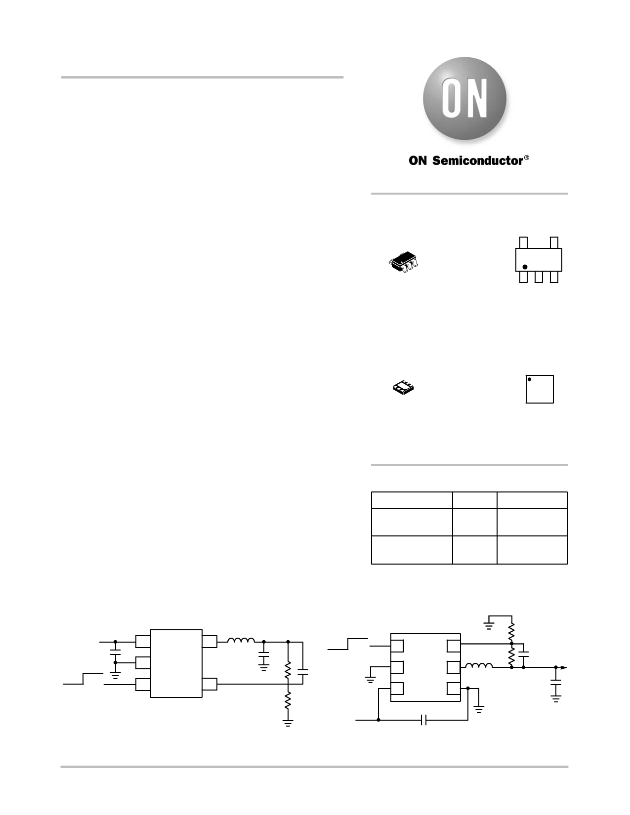
VIN
CIN
OFF ON
1 VIN LX 5
2 GND
3 EN
FB 4
L
COUT
Figure 1. Typical Application − TSOP−5
VOUT
OFF ON
R1 Cff
R2
VIN
1 EN FB 6
2 GND LX 5
R2
2.2 mH R1
3 VIN GND 4
4.7 mF
18 pF
VOUT
10 mF
Figure 2. Typical Application − UDFN6
© Semiconductor Components Industries, LLC, 2006
July, 2006 − Rev. 4
1
Publication Order Number:
NCP1521/D
1 page 
NCP1521
100
90
80
70
60
50
40
30
20
10
0
2.7
EN = VIN
IOUT = 0 mA
3.2 3.7 4.2 4.7
VIN, INPUT VOLTAGE (V)
5.2
5.7
Figure 7. Quiescent Current vs. Supply Voltage
100
90
80
70
60
50
40
30
20
10
0
−40
−20
VIN = 5.5 V
VIN = 2.7 V
0 20 40 60
TEMPERATURE (°C)
80 100
Figure 8. Quiescent Current vs. Temperature
1.0
EN = VIN
0.8 IOUT = 0 mA
0.6
0.4
0.2
0
2.7 3.2 3.7 4.2 4.7
VIN, INPUT VOLTAGE (V)
Figure 9. Shutdown Current vs. Supply Voltage
100
95
TA = −40°C
TA = 25°C
90
85
80 TA = 85°C
75
70
0 100 200 300 400 500 600
IOUT, OUTPUT CURRENT (mA)
Figure 10. Efficiency vs. Output Current
(VOUT = 1.8 V, VIN = 3.6 V)
100
90 TA = −40°C
TA = 25°C
80
70
TA = 85°C
60
50
0 100 200 300 400 500 600
IOUT, OUTPUT CURRENT (mA)
Figure 11. Efficiency vs. Output Current
(VOUT = 0.9 V, VIN = 3.6 V)
100
95 TA = −40°C
90
TA = 25°C
TA = 85°C
85
80
75
70
0 100 200 300 400 500 600
IOUT, OUTPUT CURRENT (mA)
Figure 12. Efficiency vs. Output Current
(VOUT = 3.3 V, VIN = 4.5 V)
http://onsemi.com
5
5 Page 
NCP1521
Table 3. List of Inductor
FDK
TDK
Taiyo Yuden
Coil craft
MIPW3226 Series
VLF3010AT Series
LQ CBL2012
DO1605−T Series
LPO3010
Output Capacitor Selection
Selecting the proper output capacitor is based on the
desired output ripple voltage. Ceramic capacitors with low
ESR values will have the lowest output ripple voltage and
are strongly recommended. The output capacitor requires
either an X7R or X5R dielectric.
The output ripple voltage in PWM mode is given by:
ǒ ǓDVOUT + DIL
4
1
fSW−3
) ESR (eq. 6)
COUT
In PFM mode (at light load), the output voltage is
regulated by pulse frequency modulation. The output
voltage ripple is independent of the output capacitor value.
It is set by the threshold of PFM comparator.
Table 4. List of Output Capacitor
Murata
Taiyo Yuden
TDK
GRM188R60J475KE
GRM21BR60J106ME19L
GRM188R60OJ106ME
JMK212BY475MG
JMK212BJ106MG
C2012X5ROJ475KB
C2012X5ROJ226M
C2012X5ROJ106K
4.7 mF
10 mF
10 mF
4.7 mF
10 mF
4.7 mF
22 mF
10 mF
Feed−Forward Capacitor Selection
The feed−forward capacitor sets the feedback loop
response and is critical to obtain good loop stability.
Given that the compensation is internally fixed, a fixed
18 pF or higher ceramic capacitor is needed. Choose a
small ceramic capacitor X7R or X5R or COG dielectric.
http://onsemi.com
11
11 Page | ||
| Páginas | Total 17 Páginas | |
| PDF Descargar | [ Datasheet NCP1521.PDF ] | |
Hoja de datos destacado
| Número de pieza | Descripción | Fabricantes |
| NCP152 | Low Dropout Voltage Regulator | ON Semiconductor |
| NCP1521 | Adjustable Output Voltage Step-Down Converter | ON Semiconductor |
| NCP1521B | Step-Down DC-DC Converter | ON Semiconductor |
| NCP1522 | Adjustable Output Voltage Step-Down Converter | ON Semiconductor |
| Número de pieza | Descripción | Fabricantes |
| SLA6805M | High Voltage 3 phase Motor Driver IC. |
Sanken |
| SDC1742 | 12- and 14-Bit Hybrid Synchro / Resolver-to-Digital Converters. |
Analog Devices |
|
DataSheet.es es una pagina web que funciona como un repositorio de manuales o hoja de datos de muchos de los productos más populares, |
| DataSheet.es | 2020 | Privacy Policy | Contacto | Buscar |