|
|
|
PDF AD5666 Data sheet ( Hoja de datos )
| Número de pieza | AD5666 | |
| Descripción | 16-Bit DAC | |
| Fabricantes | Analog Devices | |
| Logotipo | ||
Hay una vista previa y un enlace de descarga de AD5666 (archivo pdf) en la parte inferior de esta página. Total 28 Páginas | ||
|
No Preview Available !
www.DataSheet4U.com
Quad, 16-Bit DAC with 5 ppm/°C
On-Chip Reference in 14-Lead TSSOP
AD5666
FEATURES
Low power quad 16-bit DAC
14-lead TSSOP
On-chip 1.25 V/2.5 V, 5 ppm/°C reference
Power down to 400 nA @ 5 V, 200 nA @ 3 V
2.7 V to 5.5 V power supply
Guaranteed monotonic by design
Power-on reset to zero scale or midscale
3 power-down functions
Hardware LDAC with LDAC override function
CLR function to programmable code
SDO daisy-chaining option
Rail-to-rail operation
APPLICATIONS
Process control
Data acquisition systems
Portable battery-powered instruments
Digital gain and offset adjustment
Programmable voltage and current sources
Programmable attenuators
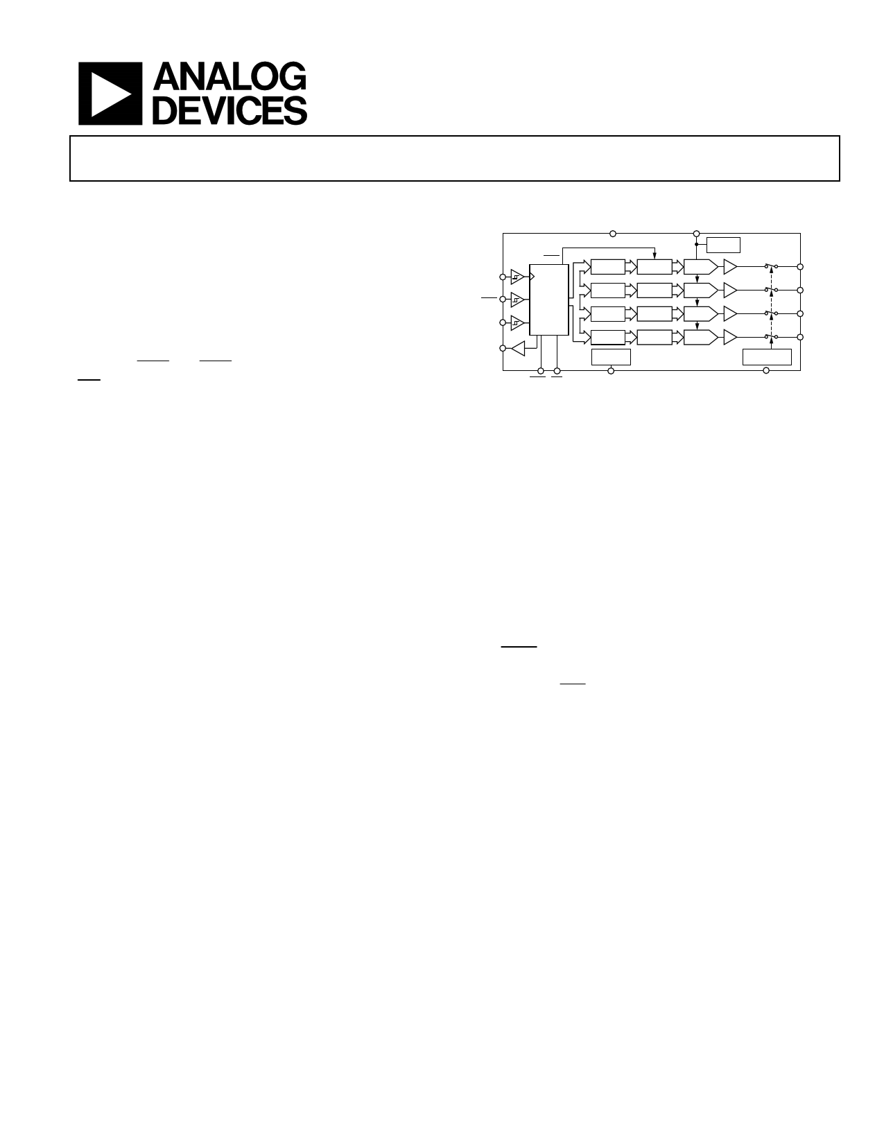
FUNCTIONAL BLOCK DIAGRAM
AD5666
LDAC
SCLK
SYNC
INTERFACE
LOGIC
DIN
SDO
VDD
VREFIN/VREFOUT
INPUT
REGISTER
DAC
REGISTER
INPUT
REGISTER
DAC
REGISTER
INPUT
REGISTER
DAC
REGISTER
INPUT
REGISTER
POWER-ON
RESET
DAC
REGISTER
1.25V/2.5V
REF
STRING
DAC A
BUFFER
STRING
DAC B
BUFFER
STRING
DAC C
BUFFER
STRING
DAC D
BUFFER
POWER-DOWN
LOGIC
LDAC CLR
POR
Figure 1.
GND
VOUTA
VOUTB
VOUTC
VOUTD
GENERAL DESCRIPTION
The AD5666 is a low power, quad, 16-bit, buffered voltage-
output DAC. The part operates from a single 2.7 V to 5.5 V
supply and is guaranteed monotonic by design.
The AD5666 has an on-chip reference with an internal gain of 2.
The AD5666-1 has a 1.25 V 5 ppm/°C reference, giving a full-scale
output of 2.5 V; the AD5666-2 has a 2.5 V 5 ppm/°C reference,
giving a full-scale output of 5 V. The on-board reference is off at
power-up, allowing the use of an external reference. The internal
reference is turned on by writing to the DAC.
The part incorporates a power-on reset circuit that ensures that
the DAC output powers up to 0 V (POR pin low) or to midscale
(POR pin high) and remains powered up at this level until a valid
write takes place. The part contains a power-down feature that
reduces the current consumption of the device to 400 nA at 5 V
and provides software-selectable output loads while in power-down
mode for any or all DAC channels.
The outputs of all DACs can be updated simultaneously using
the LDAC function, with the added functionality of user-select-
able DAC channels to simultaneously update. There is also an
asynchronous CLR that clears all DACs to a software-selectable
code—0 V, midscale, or full scale.
The AD5666 utilizes a versatile 3-wire serial interface that operates
at clock rates of up to 50 MHz and is compatible with standard
SPI®, QSPI™, MICROWIRE™, and DSP interface standards. The
on-chip precision output amplifier enables rail-to-rail output
swing.
PRODUCT HIGHLIGHTS
1. Quad, 16-bit DAC.
2. On-chip 1.25 V/2.5 V, 5 ppm/°C reference.
3. Available in 14-lead TSSOP.
4. Selectable power-on reset to 0 V or midscale.
5. Power-down capability. When powered down, the DAC
typically consumes 200 nA at 3 V and 400 nA at 5 V.
Rev. A
Information furnished by Analog Devices is believed to be accurate and reliable. However, no
responsibility is assumed by Analog Devices for its use, nor for any infringements of patents or other
rights of third parties that may result from its use. Specifications subject to change without notice. No
license is granted by implication or otherwise under any patent or patent rights of Analog Devices.
Trademarksandregisteredtrademarksarethepropertyoftheirrespectiveowners.
One Technology Way, P.O. Box 9106, Norwood, MA 02062-9106, U.S.A.
Tel: 781.329.4700
www.analog.com
Fax: 781.461.3113
© 2005 Analog Devices, Inc. All rights reserved.
1 page 
AD5666
VDD = 2.7 V to 3.6 V, RL = 2 kΩ to GND, CL = 200 pF to GND, VREFIN = VDD. All specifications TMIN to TMAX, unless otherwise noted.
Table 2.
Parameter
STATIC PERFORMANCE2
Resolution
Relative Accuracy
Differential Nonlinearity
Zero-Code Error
Zero-Code Error Drift
Full-Scale Error
Gain Error
Gain Temperature
Coefficient
Offset Error
DC Power Supply Rejection
Ratio
DC Crosstalk
(External Reference)
DC Crosstalk
(Internal Reference)
OUTPUT CHARACTERISTICS3
Output Voltage Range
Capacitive Load Stability
DC Output Impedance
Short-Circuit Current
Power-Up Time
REFERENCE INPUTS
Reference Input Voltage
Reference Current
Reference Input Range
Reference Input Impedance
REFERENCE OUTPUT
Output Voltage
Reference TC3
Reference Output
Impedance
LOGIC INPUTS3
Input Current
Input Low Voltage, VINL
Input High Voltage, VINH
Pin Capacitance
LOGIC OUTPUTS (SDO)3
Output Low Voltage, VOL
Output High Voltage, VOH
High Impedance Leakage
Current
High Impedance Leakage
Current
A Grade1
Min Typ Max
16
±32
±1
19
±2
−0.2 −1
±1
±2.5
±1 ±9
–80
10
5
10
25
10
0 VDD
2
10
0.5
30
4
VDD
40 50
0 VDD
14.6
1.247
±5
7.5
1.253
±15
2
3
VDD −
0.5
2
±3
0.8
0.4
±0.25
B Grade1
Min Typ Max
16
±16
±1
19
±2
−0.2 −1
±1
±2.5
±1 ±9
–80
10
5
10
25
10
0 VDD
2
10
0.5
30
4
VDD
40 50
0 VDD
14.6
1.247
±5
7.5
1.253
±15
2
3
VDD −
0.5
2
±3
0.8
0.4
±0.25
Unit
Bits
LSB
LSB
mV
μV/°C
% FSR
% FSR
ppm
mV
dB
μV
μV/mA
μV
μV
μV/mA
V
nF
nF
Ω
mA
μs
V
μA
kΩ
V
ppm/°C
kΩ
μA
V
V
pF
V
μA
pF
Conditions/Comments
See Figure 5
Guaranteed monotonic by design (see Figure 6)
All 0s loaded to DAC register (see Figure 13)
All 1s loaded to DAC register (see Figure 12)
Of FSR/°C
VDD ± 10%
Due to full-scale output change,
RL = 2 kΩ to GND or VDD
Due to load current change
Due to powering down (per channel)
Due to full-scale output change,
RL = 2 kΩ to GND or VDD
Due to load current change
RL = ∞
RL = 2 kΩ
VDD = 3 V coming out of power-down mode
Coming out of power-down VDD = 3 V
VREF = VDD = 3.6 V
Per DAC channel
At ambient
VDD = 3 V
VDD = 3 V
ISINK = 2 mA
ISOURCE = 2 mA
Rev. A | Page 5 of 28
5 Page 
PIN CONFIGURATION AND FUNCTION DESCRIPTIONS
LDAC 1
SYNC 2
VDD 3
VOUTA 4
VOUTC 5
POR 6
VREFIN/VREFOUT 7
AD5666
TOP VIEW
(Not to Scale)
14 SCLK
13 DIN
12 GND
11 VOUTB
10 VOUTD
9 CLR
8 SDO
Figure 5. 14-Lead TSSOP (RU-14)
AD5666
Table 6. Pin Function Descriptions
Pin No.
Mnemonic
Description
1 LDAC
2 SYNC
Pulsing this pin low allows any or all DAC registers to be updated if the input registers have new data.
This allows all DAC outputs to simultaneously update. Alternatively, this pin can be tied permanently low.
Active Low Control Input. This is the frame synchronization signal for the input data. When SYNC goes
low, it powers on the SCLK and DIN buffers and enables the input shift register. Data is transferred in
on the falling edges of the next 32 clocks. If SYNC is taken high before the 32nd falling edge, the rising
edge of SYNC acts as an interrupt and the write sequence is ignored by the device.
3 VDD
Power Supply Input. These parts can be operated from 2.7 V to 5.5 V, and the supply should be decoupled
with a 10 μF capacitor in parallel with a 0.1 μF capacitor to GND.
4 VOUTA
Analog Output Voltage from DAC A. The output amplifier has rail-to-rail operation.
5 VOUTC
Analog Output Voltage from DAC C. The output amplifier has rail-to-rail operation.
6 POR
Power-on Reset Pin. Tying this pin to GND powers up the part to 0 V. Tying this pin to VDD powers up
the part to midscale.
7
VREFIN/VREFOUT
The AD5666 has a common pin for reference input and reference output. When using the internal
reference, this is the reference output pin. When using an external reference, this is the reference input
pin. The default for this pin is as a reference input.
8 SDO
Serial Data Output. Can be used for daisy-chaining a number of these devices together or for reading
back the data in the shift register for diagnostic purposes. The serial data is transferred on the rising edge
of SCLK and is valid on the falling edge of the clock.
9 CLR
Asynchronous Clear Input. The CLR input is falling edge sensitive. When CLR is low, all LDAC pulses are
ignored. When CLR is activated, the input register and the DAC register are updated with the data
contained in the CLR code register—zero, midscale, or full scale. Default setting clears the output to 0 V.
10 VOUTD
11 VOUTB
12 GND
13 DIN
14 SCLK
Analog Output Voltage from DAC D. The output amplifier has rail-to-rail operation.
Analog Output Voltage from DAC B. The output amplifier has rail-to-rail operation.
Ground Reference Point for All Circuitry on the Part.
Serial Data Input. This device has a 32-bit shift register. Data is clocked into the register on the falling
edge of the serial clock input.
Serial Clock Input. Data is clocked into the input shift register on the falling edge of the serial clock input.
Data can be transferred at rates of up to 50 MHz.
Rev. A | Page 11 of 28
11 Page | ||
| Páginas | Total 28 Páginas | |
| PDF Descargar | [ Datasheet AD5666.PDF ] | |
Hoja de datos destacado
| Número de pieza | Descripción | Fabricantes |
| AD5660 | 12-/14-/16-Bit nanoDAC | Analog Devices |
| AD5662 | 2.7 V to 5.5 V 250 uA Rail-to-Rail Output 16-Bit DAC D/A | Analog Devices |
| AD5663 | Dual 16-Bit nanoDAC | Analog Devices |
| AD5663R | (AD5623R - AD5663R) nanoDAC | Analog Devices |
| Número de pieza | Descripción | Fabricantes |
| SLA6805M | High Voltage 3 phase Motor Driver IC. |
Sanken |
| SDC1742 | 12- and 14-Bit Hybrid Synchro / Resolver-to-Digital Converters. |
Analog Devices |
|
DataSheet.es es una pagina web que funciona como un repositorio de manuales o hoja de datos de muchos de los productos más populares, |
| DataSheet.es | 2020 | Privacy Policy | Contacto | Buscar |