|
|
PDF SCG9800 Data sheet ( Hoja de datos )
| Número de pieza | SCG9800 | |
| Descripción | 8-BIT MICROCONTROLLER | |
| Fabricantes | SCS | |
| Logotipo |  |
|
Hay una vista previa y un enlace de descarga de SCG9800 (archivo pdf) en la parte inferior de esta página. Total 29 Páginas | ||
|
No Preview Available !
www.DataSheet4U.com
SCG9800
8-BIT MICROCONTROLLER
SCG9800 Microcontroller Specification
FEATURE SUMMARY
Technology
− CMOS technology.
CPU
−
−
8-bit CPU core.
128 powerful and easy-to-use
instruction set.
Memory
− Internal RAM: 240 x 8
− Memory is organized as 16K-byte
page.
− External memory access of up to
1M x 8, can be both ROM and RAM.
I/O Structure
− Memory mapped I/O structure.
Oscillation Frequency
− RC Oscillator for the main system
clock up to 4MHz, instruction cycle
~0.5us.
− Subsystem clock frequency of
32.768kHz for real time timer.
Power Down
− Stop mode (stop main and
subsystem clock to core)
− Sleep mode (stop main system
clock only)
Interrupts
− 2 timer interrupts.
− 1 real time interrupt.
− 1 external event interrupt.
− 1 software interrupt.
I/O Ports
− 1 8-bit programmable I/O port.
− 1 2-bit output port.
Timer
−
−
−
2 8-bit pre-scalar auto reload timers
which can be cascaded to form one
16-bit timer.
1 real time timer.
1 watch dog timer.
Operating Voltage
− 2.4V to 5.5V.
Score Concept Semiconductor Ltd.
1
Sept 2000
1 page 
SCG9800
8-BIT MICROCONTROLLER
Interrupt Mask Flag (I)
The flag will be set to 1 when entering an interrupt service routine. By that
time, all other interrupt events will be pending.
After exiting from the interrupt service routine, this interrupt mask flag will be
cleared to 0. Then interrupt handling will be resumed.
Memory
By connecting PAD_EXT_ADDR to HIGH, external memory access of 512K bytes is allowed.
In addition, setting bit5 of the internal register TCONG will expand memory access to another
512K bytes. This extra external memory block can be RAM or ROM. For this ROM-less chip,
memory is arranged in 16K-byte page size each. Therefore, there can have 32 pages for
512K bytes of memory space. Regarding the instruction pointer, it is organized as iPAGE:PC
for instruction fetch.
Change of program flow between pages is by modifying the PAGE register and then followed
by executing a JMP or CALL instruction. These two instructions will load the PAGE register to
iPAGE and change the content in PC for long JMP or CALL instruction. It does not need to
change the PAGE register if it is a short JMP/CALL (i.e. JMP/CALL within page) because the
PAGE register is normally the same as the iPAGE register. To exit a subroutine, long or short
return type must be specified for long or short CALL respectively.
The microcontroller has 240 bytes internal RAM data storage of address $10-$FF. This area
includes stack frame and data memory. The stack frame is usually initialized at the highest
RAM address location, i.e. $FF.
Oscillation Circuits
Main system and subsystem oscillation circuitry generates the internal clock signal for the
CPU and other hardware timings. The main system clock uses the RC oscillation source. The
operating frequency is up to 4 MHz. This clock is for the CPU and the two timers.
The subsystem clock is for the real time signals. It uses a 32.768 kHz crystal. It has to be tied
to a voltage level, either HIGH or LOW, if the real time timer and the watch dog timer are not
used.
Power Down
The microcontroller supports power down mode for saving power.
Executing a STOP instruction will stop both main system and subsystem clock to the core to
save most of the microcontroller power. To enter sleep mode, execute a SLEEP instruction
will stop the system clock only.
Only an external interrupt will release the microcontroller from STOP mode if external
interrupt enable bit is set to 1. For SLEEP mode, the microcontroller will be awoken every 0.5
sec or by the external interrupt if corresponding enable bit is set to 1.
Score Concept Semiconductor Ltd.
5
Sept 2000
5 Page 
SCG9800
8-BIT MICROCONTROLLER
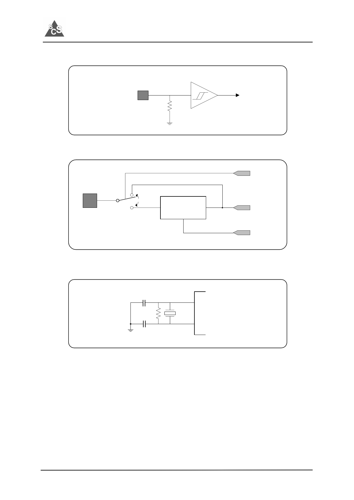
INT
Schmitt input
Figure 8. Pad type 4 (external interrupt)
RC pad
Test=1
Test=0
RC circuitry
Figure 9. Pad type 5 (RC oscillation pad)
Test
Clock out
enable
47pF
10MΩ
47pF
CLK32I
32.768
kHz
CLK32O
Figure 10. Pad type 6 (Clock circuit)
Score Concept Semiconductor Ltd.
11
Sept 2000
11 Page | ||
| Páginas | Total 29 Páginas | |
| PDF Descargar | [ Datasheet SCG9800.PDF ] | |
Hoja de datos destacado
| Número de pieza | Descripción | Fabricantes |
| SCG9800 | 8-BIT MICROCONTROLLER | SCS |
| Número de pieza | Descripción | Fabricantes |
| SLA6805M | High Voltage 3 phase Motor Driver IC. |
Sanken |
| SDC1742 | 12- and 14-Bit Hybrid Synchro / Resolver-to-Digital Converters. |
Analog Devices |
|
DataSheet.es es una pagina web que funciona como un repositorio de manuales o hoja de datos de muchos de los productos más populares, |
| DataSheet.es | 2020 | Privacy Policy | Contacto | Buscar |
