|
|
|
PDF ZL50073 Data sheet ( Hoja de datos )
| Número de pieza | ZL50073 | |
| Descripción | 32 K Channel Digital Switch | |
| Fabricantes | Zarlink Semiconductor | |
| Logotipo | ||
Hay una vista previa y un enlace de descarga de ZL50073 (archivo pdf) en la parte inferior de esta página. Total 30 Páginas | ||
|
No Preview Available !
www.DataSheet4U.com
ZL50073
32 K Channel Digital Switch with High Jitter
Tolerance, Rate Conversion per Group of
4 Streams (8, 16, 32 or 64 Mbps),
and 128 Inputs and 128 Outputs
Data Sheet
Features
April 2005
• 32,768 channel x 32,768 channel non-blocking
digital Time Division Multiplex (TDM) switch at
65.536 Mbps, 32.768 Mbps and 16.384 Mbps or
using a combination of rates
• 16,384 channel x 16,384 channel non-blocking
digital TDM switch at 8.192 Mbps
• High jitter tolerance with multiple input clock
sources and frequencies
• Up to 128 serial TDM input streams, divided into
32 groups with 4 input streams per group
• Up to 128 serial TDM output streams, divided into
32 groups with 4 output streams per group
• Per-group input and output data rate conversion
selection at 65.536 Mbps, 32.768 Mbps,
16.384 Mbps and 8.192 Mbps. Input and output
data group rates can differ
• Per-group input bit delay for flexible sampling
point selection
• Per-group output fractional bit advancement
• Four sets of output timing signals for interfacing
additional devices
• Per-channel A-Law/µ-Law Translation
Ordering Information
ZL50073GAC
484 Ball PBGA
-40°C to +85°C
• Per-channel constant or variable throughput delay
for frame integrity and low latency applications
• Per-stream Bit Error Rate (BER) test circuits
• Per-channel high impedance output control
• Per-channel force high output control
• Per-channel message mode
• Control interface compatible with Intel and
Motorola Selectable 32 bit and 16 bit non-
multiplexed buses
• Connection Memory block programming
• Supports ST-BUS and GCI-Bus standards for
input and output timing
• IEEE 1149.1 (JTAG) test port
• 3.3 V I/O with 5 V tolerant inputs; 1.8 V core
voltage
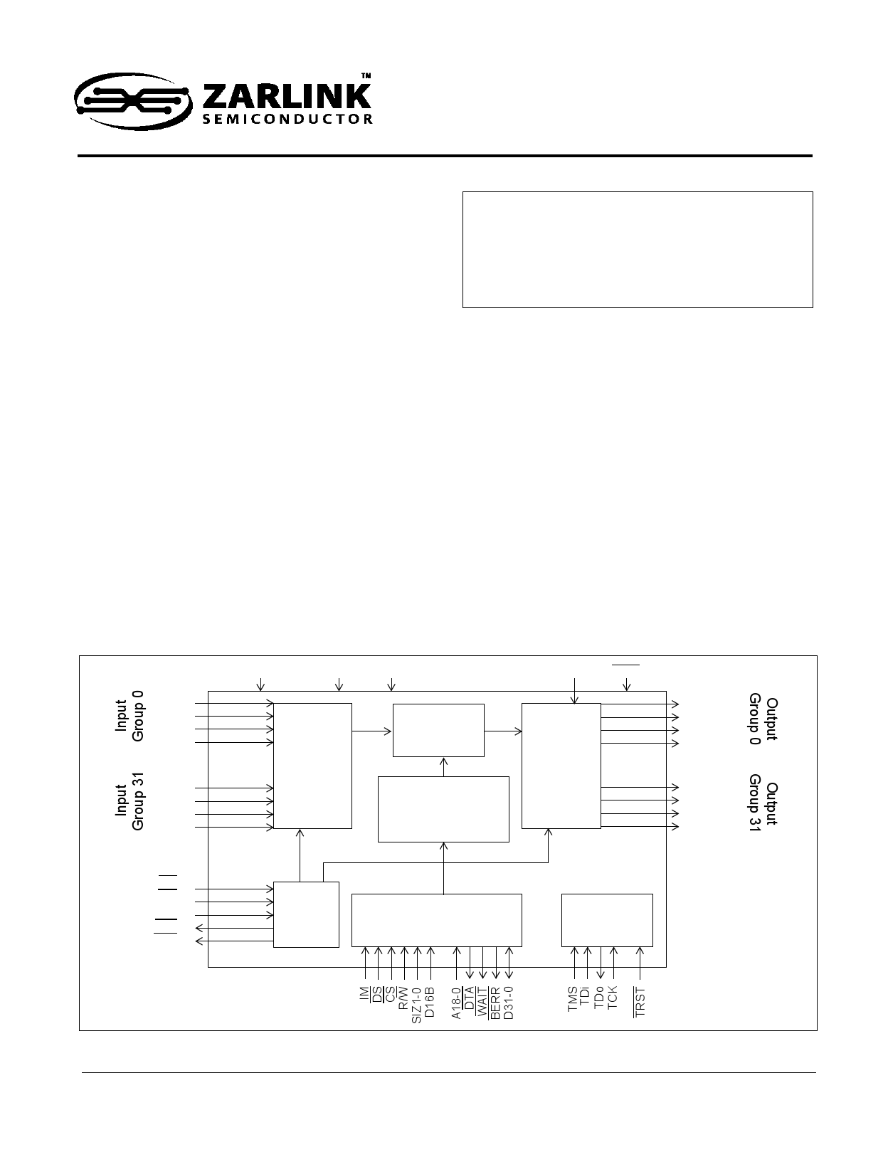
STiA0
STiB0
STiC0
STiD0
:
:
STiA31
STiB31
STiC31
STiD31
FPi2-0
CKi2-0
CK_SEL1-0
FPo3-0
CKo3-0
VDD_CORE VDD_IO VSS
ODE PWR
S/P
Converter
Input
Timing
Data Memory
P/S
Converter
Connection Memory
Output
Timing
Timing
Microprocessor Interface
and Control Registers
Test Access
Port
SToA0
SToB0
SToC0
SToD0
:
:
SToA31
SToB31
SToC31
SToD31
Figure 1 - ZL50073 Functional Block Diagram
1
Zarlink Semiconductor Inc.
Zarlink, ZL and the Zarlink Semiconductor logo are trademarks of Zarlink Semiconductor Inc.
Copyright 2004-2005, Zarlink Semiconductor Inc. All Rights Reserved.
1 page 
ZL50073
Data Sheet
List of Figures
Figure 1 - ZL50073 Functional Block Diagram . . . . . . . . . . . . . . . . . . . . . . . . . . . . . . . . . . . . . . . . . . . . . . . . . . . . 1
Figure 2 - 32 K x 32 K Channel Basic Switch Configuration . . . . . . . . . . . . . . . . . . . . . . . . . . . . . . . . . . . . . . . . . 15
Figure 3 - ZL50073 32 K x 32 K Channel and Stream Provisioning Example at Multiple Rates . . . . . . . . . . . . . . 17
Figure 4 - Input and Output Data Rate Conversion Example. . . . . . . . . . . . . . . . . . . . . . . . . . . . . . . . . . . . . . . . . 18
Figure 5 - Input Sampling Point Delay Programming. . . . . . . . . . . . . . . . . . . . . . . . . . . . . . . . . . . . . . . . . . . . . . . 20
Figure 6 - Output Bit Advancement Timing . . . . . . . . . . . . . . . . . . . . . . . . . . . . . . . . . . . . . . . . . . . . . . . . . . . . . . 21
Figure 7 - Data Throughput Delay for Constant Delay. . . . . . . . . . . . . . . . . . . . . . . . . . . . . . . . . . . . . . . . . . . . . . 23
Figure 8 - Data Throughput Delay for Variable Delay . . . . . . . . . . . . . . . . . . . . . . . . . . . . . . . . . . . . . . . . . . . . . . 23
Figure 9 - Example PRBS Timeslot Insertion. . . . . . . . . . . . . . . . . . . . . . . . . . . . . . . . . . . . . . . . . . . . . . . . . . . . . 25
Figure 10 - Read Cycle Operation . . . . . . . . . . . . . . . . . . . . . . . . . . . . . . . . . . . . . . . . . . . . . . . . . . . . . . . . . . . . . 29
Figure 11 - Write Cycle Operation . . . . . . . . . . . . . . . . . . . . . . . . . . . . . . . . . . . . . . . . . . . . . . . . . . . . . . . . . . . . . 30
Figure 12 - Frame Pulse Input and Clock Input . . . . . . . . . . . . . . . . . . . . . . . . . . . . . . . . . . . . . . . . . . . . . . . . . . . 54
Figure 13 - Frame Skew Timing Diagram . . . . . . . . . . . . . . . . . . . . . . . . . . . . . . . . . . . . . . . . . . . . . . . . . . . . . . . 55
Figure 14 - ST-Bus Frame Pulse and Clock Output Timing . . . . . . . . . . . . . . . . . . . . . . . . . . . . . . . . . . . . . . . . . . 57
Figure 15 - GCI Frame Pulse and Clock Output Timing . . . . . . . . . . . . . . . . . . . . . . . . . . . . . . . . . . . . . . . . . . . . 57
Figure 16 - Serial Data Timing to CKi . . . . . . . . . . . . . . . . . . . . . . . . . . . . . . . . . . . . . . . . . . . . . . . . . . . . . . . . . . 59
Figure 17 - Serial Data Timing to CKo . . . . . . . . . . . . . . . . . . . . . . . . . . . . . . . . . . . . . . . . . . . . . . . . . . . . . . . . . . 61
Figure 18 - CKo to other CKo Skew. . . . . . . . . . . . . . . . . . . . . . . . . . . . . . . . . . . . . . . . . . . . . . . . . . . . . . . . . . . . 62
Figure 19 - Microprocessor Bus Interface Timing . . . . . . . . . . . . . . . . . . . . . . . . . . . . . . . . . . . . . . . . . . . . . . . . . 64
Figure 20 - Intel Mode Timing . . . . . . . . . . . . . . . . . . . . . . . . . . . . . . . . . . . . . . . . . . . . . . . . . . . . . . . . . . . . . . . . 64
Figure 21 - IEEE 1149.1 Test Port & PWR Reset Timing. . . . . . . . . . . . . . . . . . . . . . . . . . . . . . . . . . . . . . . . . . . . 65
5
Zarlink Semiconductor Inc.
5 Page 
ZL50073
Data Sheet
Pin Description (continued)
Pin
D4, F4, G3, G2, G1, L2, N3,
T1, U2, T6, V5, AA3, W7,
AA7, W10, Y11, Y12, AB17,
AA18, W18, V19, AA22,
U21, N17, P22, L21, L17,
H20, D22, E20, C20, D16
W12
AA13
J2, G21
K3, K19
Name
SToD0-31
CKi0
FPi0
CKi1-2
FPi1-2
Description
Serial TDM Output Data ’D’ Streams (5 V Tolerant, 3.3 V
Tri-state Slew-Rate Controlled Outputs)
The data rate of these output streams can be selected in a group of
4 to be either 8.192 Mbps or 16.384 Mbps. The stream is unused
when its output group rate is 65.536 Mbps or 32.678 Mbps. Refer to
Section 1.4 for rate programming options.
The data streams can be selected to be either inverted or
non-inverted, programmed by the Group Control Registers (Section
14.4).
Unused outputs are tristated and may be left unconnected.
ST-BUS/GCI-Bus Clock Input (5 V Tolerant Schmitt-Triggered
Input)
This pin accepts an 8.192 MHz, 16.384 MHz, 32.678 MHz or
65.536 MHz clock. This clock must be provided for correct
operation of the ZL50073. The frequency of the CKi0 input is
selected by the CK_SEL1-0 inputs. The active clock edge may be
either rising or falling, programmed by the Input Clock Control
Register (Section 14.5).
ST-BUS/GCI-Bus Frame Pulse Input (5 V Tolerant Input)
This pin accepts the 8 kHz frame pulse which marks the frame
boundary of the TDM data streams. The pulse width is nominally
one CKi0 clock period (assuming ST-BUS mode) selected by the
CK_SEL1-0 inputs. The active state of the frame pulse may be
either high or low, programmed by the Input Clock Control Register
(Section 14.5).
ST-BUS/GCI-Bus Clock Inputs (5 V Tolerant Schmitt Triggered
Inputs)
These optional TDM clock inputs are at 8.192 MHz, 16.384 MHz,
32.678 MHz or 65.536 MHz. The frequency of each clock input is
automatically detected by the ZL50073. Refer to Section 2.0 for
TDM timing options. The active clock edge may be either rising or
falling, programmed by the Input Clock Control Register (Section
14.5). Unused inputs must be connected to a defined logic level.
ST-BUS/GCI-Bus Frame Pulse Inputs (5 V Tolerant Inputs)
These 8 kHz input pulses correspond to the optional CKi2-1 clock
inputs. The frame pulses mark the frame boundary of the TDM data
streams. Refer to Section 2.0 for TDM timing options. Each pulse
width is nominally one CKi clock period (assuming ST-BUS mode).
The active state of the frame pulse may be either high or low,
programmed by the Input Clock Control Register (Section 14.5).
Unused inputs must be connected to a defined logic level.
11
Zarlink Semiconductor Inc.
11 Page | ||
| Páginas | Total 30 Páginas | |
| PDF Descargar | [ Datasheet ZL50073.PDF ] | |
Hoja de datos destacado
| Número de pieza | Descripción | Fabricantes |
| ZL50070 | 24 K Channel Digital Switch | Zarlink Semiconductor |
| ZL50073 | 32 K Channel Digital Switch | Zarlink Semiconductor |
| ZL50074 | 32 K x 32 K Channel TDM Switch | Zarlink Semiconductor |
| ZL50075 | 32 K Channel Digital Switch | Zarlink Semiconductor |
| Número de pieza | Descripción | Fabricantes |
| SLA6805M | High Voltage 3 phase Motor Driver IC. |
Sanken |
| SDC1742 | 12- and 14-Bit Hybrid Synchro / Resolver-to-Digital Converters. |
Analog Devices |
|
DataSheet.es es una pagina web que funciona como un repositorio de manuales o hoja de datos de muchos de los productos más populares, |
| DataSheet.es | 2020 | Privacy Policy | Contacto | Buscar |