|
|
|
PDF IRFB4019PBF Data sheet ( Hoja de datos )
| Número de pieza | IRFB4019PBF | |
| Descripción | DIGITAL AUDIO MOSFET | |
| Fabricantes | International Rectifier | |
| Logotipo | ||
Hay una vista previa y un enlace de descarga de IRFB4019PBF (archivo pdf) en la parte inferior de esta página. Total 7 Páginas | ||
|
No Preview Available !
www.DataSheet4U.com
DIGITAL AUDIO MOSFET
PD - 97075
IRFB4019PbF
Features
• Key Parameters Optimized for Class-D Audio
Amplifier Applications
• Low RDSON for Improved Efficiency
• Low QG and QSW for Better THD and Improved
Efficiency
• Low QRR for Better THD and Lower EMI
• 175°C Operating Junction Temperature for
Ruggedness
• Can Deliver up to 200W per Channel into 8Ω Load in
Half-Bridge Configuration Amplifier
Key Parameters
VDS 150
RDS(ON) typ. @ 10V
80
Qg typ.
Qsw typ.
RG(int) typ.
13
5.1
2.4
TJ max
175
DD
V
m:
nC
nC
Ω
°C
G
S
S
D
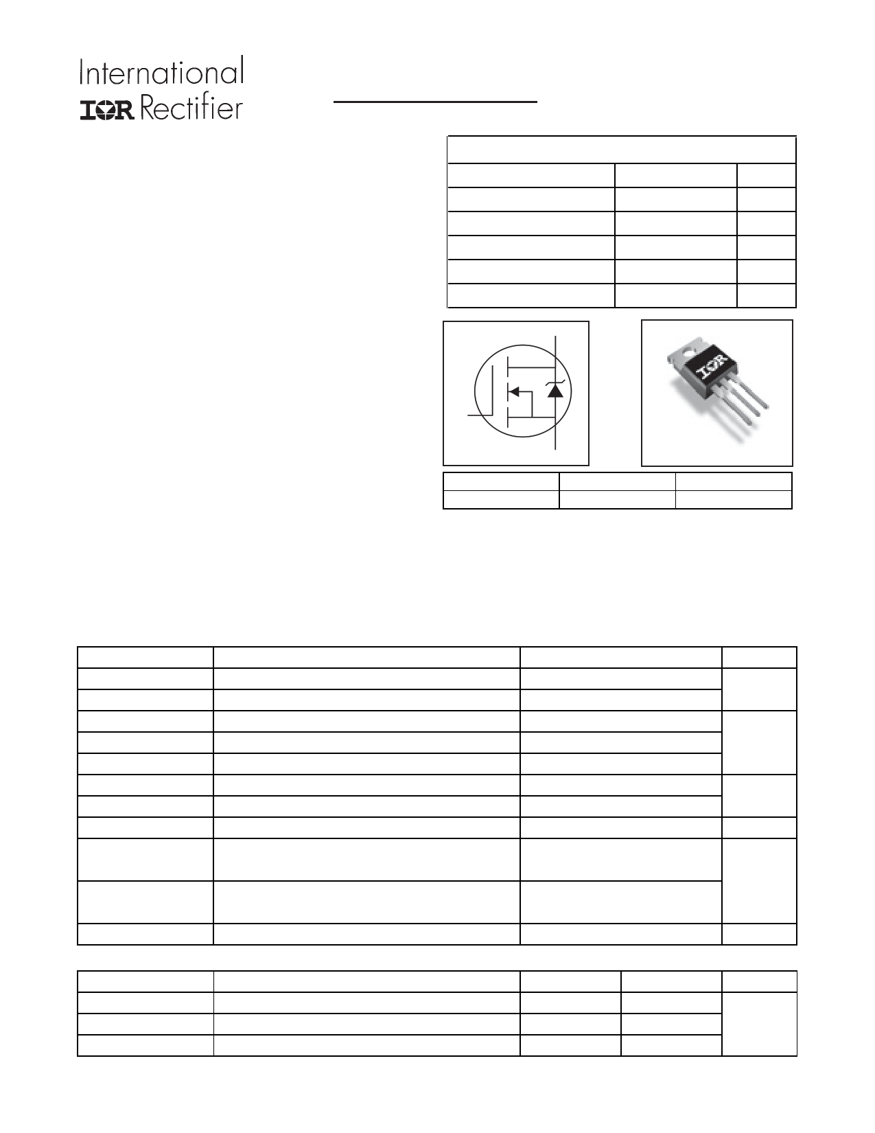
G
TO-220AB
GDS
Description
Gate
Drain
Source
This Digital Audio MOSFET is specifically designed for Class-D audio amplifier applications. This MOSFET utilizes
the latest processing techniques to achieve low on-resistance per silicon area. Furthermore, Gate charge, body-diode
reverse recovery and internal Gate resistance are optimized to improve key Class-D audio amplifier performance
factors such as efficiency, THD and EMI. Additional features of this MOSFET are 175°C operating junction
temperature and repetitive avalanche capability. These features combine to make this MOSFET a highly efficient,
robust and reliable device for ClassD audio amplifier applications.
Absolute Maximum Ratings
Parameter
VDS
VGS
ID @ TC = 25°C
ID @ TC = 100°C
IDM
PD @TC = 25°C
PD @TC = 100°C
Drain-to-Source Voltage
Gate-to-Source Voltage
Continuous Drain Current, VGS @ 10V
Continuous Drain Current, VGS @ 10V
Pulsed Drain Current c
Power Dissipation f
Power Dissipation f
TJ
TSTG
Linear Derating Factor
Operating Junction and
Storage Temperature Range
Soldering Temperature, for 10 seconds
(1.6mm from case)
Mounting torque, 6-32 or M3 screw
Max.
150
±20
17
12
51
80
40
0.5
-55 to + 175
300
10lbxin (1.1Nxm)
Units
V
A
W
W/°C
°C
Thermal Resistance
Parameter
RθJC
RθCS
RθJA
Junction-to-Case f
Case-to-Sink, Flat, Greased Surface
Junction-to-Ambient f
Notes through
are on page 2
www.irf.com
Typ.
–––
0.50
–––
Max.
1.88
–––
62
Units
°C/W
1
3/2/06
1 page 
0.5
ID = 10A
0.4
0.3
0.2
0.1
0.0
4
TJ = 125°C
TJ = 25°C
6 8 10 12 14
VGS, Gate-to-Source Voltage (V)
16
IRFB4019PbF
300
ID
250
TOP 1.3A
2.3A
BOTTOM 10A
200
150
100
50
0
25
50 75 100 125 150 175
Starting TJ, Junction Temperature (°C)
Fig 12. On-Resistance Vs. Gate Voltage
100
Fig 13. Maximum Avalanche Energy Vs. Drain Current
Duty Cycle = Single Pulse
10
0.01
0.05
0.10
1
Allowed avalanche Current vs avalanche
pulsewidth, tav, assuming ∆Τ j = 25°C and
Tstart = 150°C.
Allowed avalanche Current vs avalanche
pulsewidth, tav, assuming ∆Tj = 150°C and
Tstart =25°C (Single Pulse)
0.1
1.0E-06
1.0E-05
1.0E-04
1.0E-03
1.0E-02
1.0E-01
tav (sec)
Fig 14. Typical Avalanche Current Vs.Pulsewidth
80
TOP
Single Pulse
BOTTOM 1% Duty Cycle
ID = 10A
60
Notes on Repetitive Avalanche Curves , Figures 14, 15:
(For further info, see AN-1005 at www.irf.com)
1. Avalanche failures assumption:
Purely a thermal phenomenon and failure occurs at a
temperature far in excess of Tjmax. This is validated for
every part type.
2. Safe operation in Avalanche is allowed as long as neither
Tjmax nor Iav (max) is exceeded
40
20
0
25
50 75 100 125 150 175
Starting TJ , Junction Temperature (°C)
Fig 15. Maximum Avalanche Energy Vs. Temperature
3. Equation below based on circuit and waveforms shown in
Figures 17a, 17b.
4. PD (ave) = Average power dissipation per single
avalanche pulse.
5. BV = Rated breakdown voltage (1.3 factor accounts for
voltage increase during avalanche).
6. Iav = Allowable avalanche current.
7. ∆T = Allowable rise in junction temperature, not to exceed
Tjmax (assumed as 25°C in Figure 14, 15).
tav = Average time in avalanche.
D = Duty cycle in avalanche = tav ·f
ZthJC(D, tav) = Transient thermal resistance, see figure 11)
PD (ave) = 1/2 ( 1.3·BV·Iav) = DT/ ZthJC
Iav = 2DT/ [1.3·BV·Zth]
EAS (AR) = PD (ave)·tav
www.irf.com
5
5 Page | ||
| Páginas | Total 7 Páginas | |
| PDF Descargar | [ Datasheet IRFB4019PBF.PDF ] | |
Hoja de datos destacado
| Número de pieza | Descripción | Fabricantes |
| IRFB4019PBF | DIGITAL AUDIO MOSFET | International Rectifier |
| Número de pieza | Descripción | Fabricantes |
| SLA6805M | High Voltage 3 phase Motor Driver IC. |
Sanken |
| SDC1742 | 12- and 14-Bit Hybrid Synchro / Resolver-to-Digital Converters. |
Analog Devices |
|
DataSheet.es es una pagina web que funciona como un repositorio de manuales o hoja de datos de muchos de los productos más populares, |
| DataSheet.es | 2020 | Privacy Policy | Contacto | Buscar |