|
|
PDF S29WS064N Data sheet ( Hoja de datos )
| Número de pieza | S29WS064N | |
| Descripción | Burst Mode Flash Memory | |
| Fabricantes | SPANSION | |
| Logotipo |  |
|
Hay una vista previa y un enlace de descarga de S29WS064N (archivo pdf) en la parte inferior de esta página. Total 70 Páginas | ||
|
No Preview Available !
www.DataSheet4U.com
S29WSxxxN MirrorBit™ Flash Family
S29WS256N, S29WS128N, S29WS064N
256/128/64 Megabit (16/8/4 M x 16-Bit) CMOS 1.8 Volt-only
Simultaneous Read/Write, Burst Mode Flash Memory
Data Sheet
General Description
PRELIMINARY
The Spansion S29WS256/128/064N are MirrorbitTM Flash products fabricated on 110 nm process technology. These burst
mode Flash devices are capable of performing simultaneous read and write operations with zero latency on two separate
banks using separate data and address pins. They operate up to 80 MHz and use a single VCC of 1.7–1.95 volts that
makes them ideal for today’s demanding wireless applications requiring higher density, better performance and lowered
power consumption.
Distinctive Characteristics
Single 1.8 V read/program/erase (1.70–1.95 V)
110 nm MirrorBit™ Technology
Simultaneous Read/Write operation with zero
latency
32-word Write Buffer
Sixteen-bank architecture consisting of 16/8/4
Mbit for WS256N/128N/064N, respectively
Four 16 Kword sectors at both top and bottom of
memory array
254/126/62 64 Kword sectors (WS256N/128N/
064N)
Programmable burst read modes
— Linear for 32, 16 or 8 words linear read with or
without wrap-around
— Continuous sequential read mode
SecSi™ (Secured Silicon) Sector region consisting
of 128 words each for factory and customer
20-year data retention (typical)
Cycling Endurance: 100,000 cycles per sector
(typical)
RDY output indicates data available to system
Command set compatible with JEDEC standards
Hardware (WP#) protection of top and bottom
sectors
Dual boot sector configuration (top and bottom)
Offered Packages
— WS064N: 80-ball FBGA (7 mm x 9 mm)
— WS256N/128N: 84-ball FBGA (8 mm x 11.6 mm)
Low VCC write inhibit
Persistent and Password methods of Advanced
Sector Protection
Write operation status bits indicate program and
erase operation completion
Suspend and Resume commands for Program and
Erase operations
Unlock Bypass program command to reduce
programming time
Synchronous or Asynchronous program operation,
independent of burst control register settings
ACC input pin to reduce factory programming time
Support for Common Flash Interface (CFI)
Industrial Temperature range (contact factory)
Performance Characteristics
Read Access Times
Speed Option (MHz)
80
Max. Synch. Latency, ns (tIACC)
Max. Synch. Burst Access, ns (tBACC)
Max. Asynch. Access Time, ns (tACC)
Max CE# Access Time, ns (tCE)
Max OE# Access Time, ns (tOE)
69
9
70
70
11.2
66
69
11.2
70
70
11.2
54
69
13.5
70
70
13.5
Current Consumption (typical values)
Continuous Burst Read @ 66 MHz
Simultaneous Operation (asynchronous)
Program (asynchronous)
Erase (asynchronous)
Standby Mode (asynchronous)
35 mA
50 mA
19 mA
19 mA
20 µA
Typical Program & Erase Times
Single Word Programming
Effective Write Buffer Programming (VCC) Per Word
Effective Write Buffer Programming (VACC) Per Word
Sector Erase (16 Kword Sector)
Sector Erase (64 Kword Sector)
40 µs
9.4 µs
6 µs
150 ms
600 ms
Publication Number S29WSxxxN_00 Revision F Amendment 0 Issue Date October 29, 2004
1 page 
Preliminary
1 Ordering Information
The ordering part number is formed by a valid combination of the following:
S29WS 256 N 0S BA W 01 0
PACKING TYPE
0 = Tray (standard; see note 1)
2 = 7-inch Tape and Reel
3 = 13-inch Tape and Reel
MODEL NUMBER (Note 3)
(Package Ball Count, Package Dimensions, DYB Protect/Unprotect After
Power-up)
01 = 84-ball, 8 x 11.6 mm, DYB Unprotect
11 = 80-ball, 7 x 9 mm, DYB Protect
TEMPERATURE RANGE (Note 3)
W = Wireless (–25°C to +85°C)
I = Industrial (–40°C to +85°C, contact factory for availability)
PACKAGE TYPE AND MATERIAL
BA = Very Thin Fine-Pitch BGA, Lead (Pb)-free Compliant Package
BF = Very Thin Fine-Pitch BGA, Lead (Pb)-free Package
SPEED OPTION (BURST FREQUENCY)
0S = 80 MHz
0P = 66 MHz
0L = 54 MHz
PROCESS TECHNOLOGY
N = 110 nm MirrorBit™ Technology
FLASH DENSITY
256 = 256 Mb
128 = 128 Mb
064 = 64 Mb
DEVICE FAMILY
S29WS = 1.8 Volt-only Simultaneous Read/Write, Burst Mode Flash Memory
S29WSxxxN Valid Combinations (Notes 1, 2, 3)
Base Ordering
Part Number
Speed
Option
Package Type, Material, & Model
Temperature Range
Number
S29WS256N
01
11
S29WS128N
0S, 0P, 0L
BAW (Lead (Pb)-free Compliant),
BFW (Lead (Pb)-free)
01
11
S29WS064N
01
11
Packing
Type
0, 2, 3
(Note 1)
VIO Range
DYB
Power Up
State
1.70–1.95 V
Unprotect
Protect
Unprotect
Protect
Unprotect
Protect
Package Type
(Note 2)
8 mm x 11.6 mm
84-ball
MCP-Compatible
7 mm x 9 mm
80-ball
MCP-Compatible
Notes:
1. Type 0 is standard. Specify other options as required.
2. BGA package marking omits leading “S29” and packing type
designator from ordering part number.
3. For 1.5 VIO option, other boot options, or industrial temperature
range, contact your local sales office.
Valid Combinations
Valid Combinations list configurations planned to be supported in vol-
ume for this device. Consult your local sales office to confirm avail-
ability of specific valid combinations and to check on newly released
combinations.
October 29, 2004 S29WSxxxN_00_F0
S29WSxxxN MirrorBit™ Flash Family
5
5 Page 
Preliminary
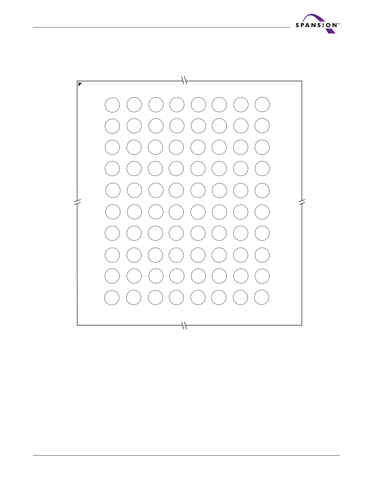
80-ball Fine-Pitch Ball Grid Array, 64 Mb
(Top View, Balls Facing Down,
MCP Compatible)
A1
AVD#
B1
WP#
C1
A3
D1
A2
E1
A1
F1
A0
G1
CE#f1
H1
RFU
J1
RFU
K1
RFU
A2
RFU
B2
A7
C2
A6
D2
A5
E2
A4
F2
VSS
G2
OE#
H2
DQ0
J2
DQ8
K2
RFU
A3 A4 A5
CLK RFU RFU
B3 B4 B5
RFU ACC WE#
C3 C4
C5
RFU RESET#
D3 D4
RFU
D5
A18 RDY
A20
E3 E4
A17 RFU
F3 F4
DQ1 RFU
E5
RFU
F5
RFU
G3
DQ9
G4
DQ3
G5
DQ4
H3
DQ10
J3
DQ2
H4
VCC
J4
DQ11
H5
RFU
J5
RFU
K3 K4 K5
RFU VCC RFU
A6
RFU
B6
A8
C6
A19
D6
A9
E6
A10
F6
DQ6
G6
DQ13
H6
DQ12
J6
DQ5
K6
RFU
A7
RFU
B7
A11
C7
A12
D7
A13
E7
A14
F7
RFU
G7
DQ15
H7
DQ7
J7
DQ14
K7
RFU
A8
RFU
B8
RFU
C8
A15
D8
A21
E8
RFU
F8
A16
G8
RFU
H8
VSS
J8
RFU
K8
RFU
Figure 4.3. 80-ball Fine-Pitch Ball Grid Array (S29WS064N)
October 29, 2004 S29WSxxxN_00_F0
S29WSxxxN MirrorBit™ Flash Family
11
11 Page | ||
| Páginas | Total 70 Páginas | |
| PDF Descargar | [ Datasheet S29WS064N.PDF ] | |
Hoja de datos destacado
| Número de pieza | Descripción | Fabricantes |
| S29WS064J | (S29WS064J / S29WS128J) Burst Mode Flash Memory | SPANSION |
| S29WS064N | SIMULTANEOUS READ/WRITE BURST MODE FLASH MEMORY | SPANSION |
| S29WS064N | Burst Mode Flash Memory | SPANSION |
| Número de pieza | Descripción | Fabricantes |
| SLA6805M | High Voltage 3 phase Motor Driver IC. |
Sanken |
| SDC1742 | 12- and 14-Bit Hybrid Synchro / Resolver-to-Digital Converters. |
Analog Devices |
|
DataSheet.es es una pagina web que funciona como un repositorio de manuales o hoja de datos de muchos de los productos más populares, |
| DataSheet.es | 2020 | Privacy Policy | Contacto | Buscar |
