|
|
PDF T6K14 Data sheet ( Hoja de datos )
| Número de pieza | T6K14 | |
| Descripción | COLUMN AND ROW DRIVER LSI | |
| Fabricantes | Toshiba Semiconductor | |
| Logotipo | ||
Hay una vista previa y un enlace de descarga de T6K14 (archivo pdf) en la parte inferior de esta página. Total 30 Páginas | ||
|
No Preview Available !
www.DataSheet4U.com
TOSHIBA CMOS DIGITAL INTEGRATED CIRCUIT SILICON MONOLITHIC
T6K14
T6K14
COLUMN AND ROW DRIVER LSI FOR A DOT MATRIX GRAPHIC LCD
The T6K14 is a driver for a small-to-medium-sized dot matrix
graphic LCD, especially for reflective color STN LCD. It realizes a
4-color or 4-gray-scale display. This driver can be interfaced to
Unit: mm
the MPU via an 8-bit (68/80-series) or a serial interface, and is
operated asynchronously with the MPU. Since the T6K14
contains a CR oscillator, it can generate the timing signals
required for the LCD. Since the T6K14 has 128 outputs for the
T6K14
(UBW, 5NS)
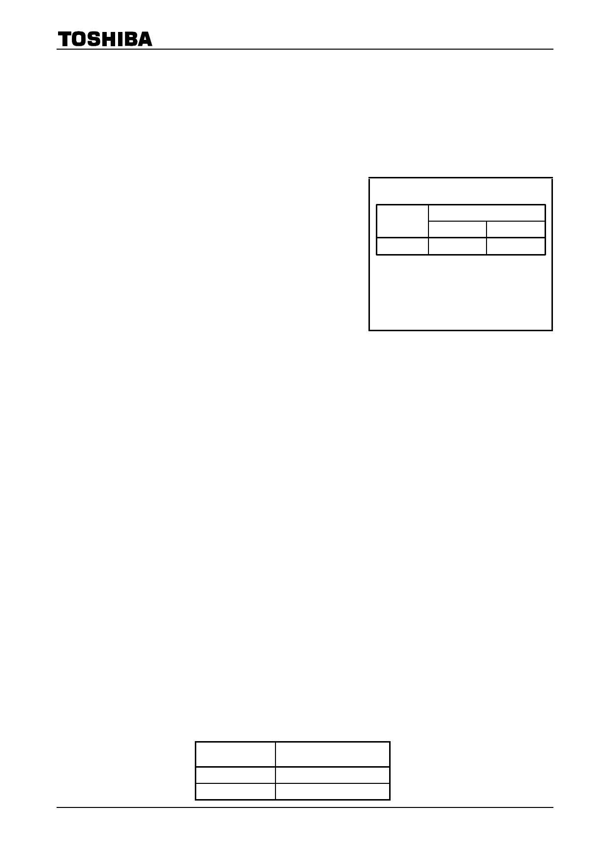
Lead Pitch
IN OUT
0.60 0.23
LCD drive (segment) signals that constitute display data, 65
outputs for the LCD drive (common) signals that constitute
Please contact with Toshiba agents for
each packaging outline dimensions.
scanning signals and 65 × 128 × 2 bits display RAM, this single
device allows you to drive an LCD panel comprised of up to 128 ×
64 dots and 128 icons with a minimize of power requirement. It
TCP (Tape Carrier Package)
has 4 gray-scale function. The display RAM of this driver is a 2
port RAM so that the MPU accesses without any wait time. It has
various power circuits such as a voltage regulators, voltage
divider resistors, a power supply op-amp, a contrast control circuit, a temperature compensation circuit, and
DC-DC converter ( ×2, ×3, ×4, ×5 ). All these circuits enable the LCD panel to be driven with a single power supply.
Features
l LCD driver output
l Built in display RAM
l Gray scale
l Word length
l Duty cycle
l Display modes
l Clock oscillator
l Power circuit
l CPU interface
l Logic operating voltage
l LCD drive voltage
l CMOS process
l Low power consumption
Condition
l Package
: 64 rows + 128 columns + 128 icons
: 65 × 128 × 2 = 16640 bits, 2-port RAM
: 4 gray-scale selectable
: 8-bit/word
: 1/2 duty (power save mode)
1/35, 1/49, 1/57, 1/65 duty selectable (normal display mode)Display mode
: Normal mode (Full display)
Power save mode (Icon display)
Stand by mode (Clock stopped)
: CR oscillator with external resistors
Low frequency operation 82 kHz oscillation for FR frequency 70 Hz (1/65 duty)
: Voltage regulator, Voltage divider, Voltage follower op-amp.
DC-DC converter (×2, ×3, ×4, ×5), Temperature compensation circuit, Contrast
control circuit.
: Interfacing with 68/80 series MPU and Serial Interface
: VDD = 2.4 to 3.3 V, VIN = 2.7 to 3.3 V
: VCC1, 2 = 6.0 to 16.5 V, if case of used the voltage Regulator, VCC2 output voltage
at 12.5 V or 11.0 V (typ.) Ta = 25°C
: ISS = 200 µA (typ.)
: VDD = 2.7 V, VIN = 2.7 V, using the DC-DC converter (×5), no data access, op-amp
on, fosc = 82 kHz (internal clock), no load, 1/65 duty, temperature compensation
circuit off.
:
Product
Package
T6K14 (×××, ×××)
JBT6K14-AS
TCP (Tape carrier package)
Gold bump chip
1 2002-01-16
1 page 
T6K14
5 2002-01-16
5 Page 
Pin Function (3)
Pin Name
MD
M/S
CL
PM
FR
SYNC
CK
I/O
Input
Input
I/O
I/O
I/O
I/O
I/O
Function
Mode detect pin for Status Read
Input for master/slave selects
● M/S = H → T6K14 is master chip
● M/S = L → T6K14 is slave chip
Input/Output for shift clock pulse
● Master mode (M/S = H) → output
● Slave mode (M/S = L) → input
Input/Output for frame signal
● Master mode (M/S = H) → output
● Slave mode (M/S = L) → input
Input/Output for display synchronous signal
● Master mode (M/S = H) → output
● Slave mode (M/S = L) → input
Input/Output for grayscale signal data
● Master mode (M/S = H) → output
● Slave mode (M/S = L) → input
Input/Output for grayscale signal data
● Master mode (M/S = H) → output
● Slave mode (M/S = L) → input
T6K14
Pin Function (4)
PS 68/80
Interface Type
/CS1 CS2 D/I
RS /WR /RD SO
SI SCK DB0 to DB7
80 series MPU (/CS1) /CS1 H
A0 A1 /WR /RD Open L/H L/H DB0 to DB7
L
H
80 series MPU (CS2)
L CS2 A0 A1 /WR /RD Open L/H L/H DB0 to DB7
H 68 series MPU
L H A0 A1 R/W E Open L/H L/H DB0 to DB7
L L/H Serial interface
L
H
L/H L/H L/H L/H SO
SI SCK
Open
Note: H denotes the VDD level; L denotes the VSS level.
11 2002-01-16
11 Page | ||
| Páginas | Total 30 Páginas | |
| PDF Descargar | [ Datasheet T6K14.PDF ] | |
Hoja de datos destacado
| Número de pieza | Descripción | Fabricantes |
| T6K11 | DOT MATRIX LCD DRIVER | Toshiba Semiconductor |
| T6K14 | COLUMN AND ROW DRIVER LSI | Toshiba Semiconductor |
| Número de pieza | Descripción | Fabricantes |
| SLA6805M | High Voltage 3 phase Motor Driver IC. |
Sanken |
| SDC1742 | 12- and 14-Bit Hybrid Synchro / Resolver-to-Digital Converters. |
Analog Devices |
|
DataSheet.es es una pagina web que funciona como un repositorio de manuales o hoja de datos de muchos de los productos más populares, |
| DataSheet.es | 2020 | Privacy Policy | Contacto | Buscar |
