|
|
PDF T7502 Data sheet ( Hoja de datos )
| Número de pieza | T7502 | |
| Descripción | Dual PCM Codec | |
| Fabricantes | Agere Systems | |
| Logotipo |  |
|
Hay una vista previa y un enlace de descarga de T7502 (archivo pdf) en la parte inferior de esta página. Total 16 Páginas | ||
|
No Preview Available !
www.DataSheet4U.com
Data Sheet
February 1998
T7502 Dual PCM Codec with Filters
Features
s +5 V only
s Automatic powerdown mode
s Low-power, latch-up-free CMOS technology
s On-chip sample and hold, autozero, and precision
voltage reference
s Differential architecture for high noise immunity
and power supply rejection
s Automatic master clock frequency selection
s 2.048 MHz or 4.096 MHz fixed data rate
s Frame sync controlled channel swapping
s Differential analog I/O
s 300 Ω output drivers
s Operating temperature range: –40 °C to +85 °C
s A-law companding
Applications
s Speakerphone
s Telephone answering device (TAD)
s POTS for ISDN
Description
The T7502 device is a single-chip, two-channel
A-law PCM codec with filters. This integrated circuit
provides analog-to-digital and digital-to-analog
conversion. It provides the transmit and receive
filtering necessary to interface a voice telephone
circuit to a time-division multiplexed (TDM) system.
The device features a differential transmit amplifier,
and the power receive amplifier is capable of driving
600 Ω differentially. PCM timing is defined by a single
frame sync pulse. This device operates in a delayed
timing mode (digital data is valid one clock cycle after
frame sync goes high). The T7502 is packaged in a
20-pin SOJ.
GSX0
VFXIN0
VFXIP0
VCM0
VFROP0
VFRON0
GSX1
VFXIN1
VFXIP1
VCM1
VFROP1
VFRON1
– FILTER
+ NETWORK
+2.4 V CHANNEL 0
ENCODER
PCM
INTERFACE
FILTER
NETWORK
DECODER
CHANNEL 1
POWERDOWN
CONTROL
INTERNAL TIMING
& CONTROL
BIAS
CIRCUITRY
&
REFERENCE
Figure 1. Block Diagram
DX
DR
GNDD
FS
MCLK
VDD (1)
GNDA (2)
5-3609.b
1 page 
Data Sheet
February 1998
T7502 Dual PCM Codec with Filters
Electrical Characteristics (continued)
dc Characteristics (continued)
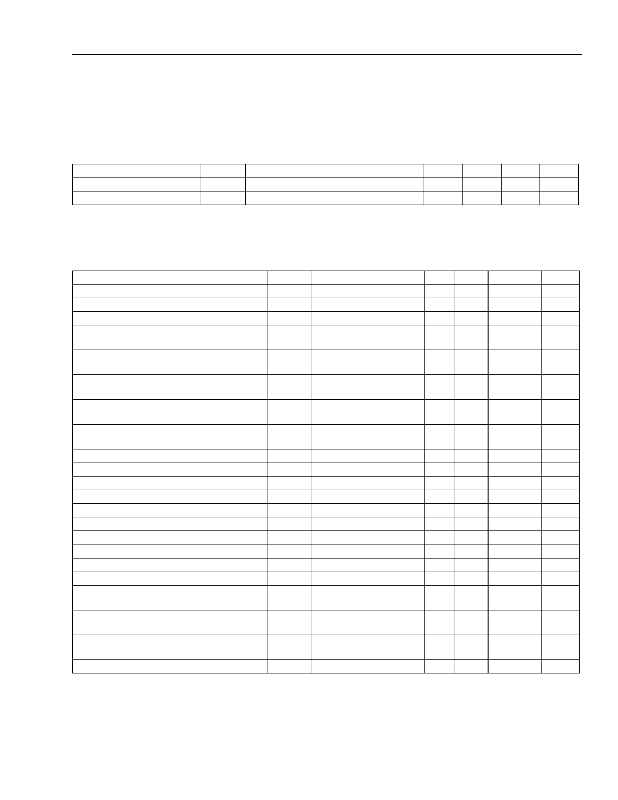
Table 3. Power Dissipation
Power measurements are made at MCLK = 4.096 MHz, outputs unloaded.
Parameter
Powerdown Current
Powerup Current
Symbol
IDDO
IDDU
Test Conditions
MCLK present and FS ≤ 0.4 V
MCLK, FS pulse present
Min Typ Max Unit
— 0.1 1 mA
— 18 25 mA
Transmission Characteristics
Table 4. Analog Interface
Parameter
Input Resistance, FSXI
Input Leakage Current, VFXI
Input Capacitance, VFXIN, VFXIP
Input Offset Voltage of Uncommitted
Op Amp, VFXIN – VFXIP
Input Common-mode Voltage Range,
VFXIN, VFXIP
Input Common-mode Rejection Ratio,
VFXIN, VFXIP
Gain Bandwidth Product (10 kHz) of Un-
committed Op Amp
Equivalent Input Noise Between VFXIN
and VFXIP at GSX
Output Voltage Range, GSX
dc Open-loop Voltage Gain, GSX
Differential Output dc Offset Voltage
Load Capacitance, GSX
Load Resistance, GSX
VCM Output Voltage Referenced to GND
VCM Output Load Capacitance
Load Resistance, VCM
Load Resistance, VFRO
Load Capacitance, VFRO
Output Resistance, VFRO
Output Voltage, VFRO
Output Leakage Current, VFRO, Power-
down
Output Voltage Swing, VFRO
Symbol
RVFXI
IBVFXI
—
—
Test Conditions
VFxI = 2.4 V
VFxI = 2.4 V
—
—
Min Typ
1.0 —
–2.4 ±0.01
—
–5 —
Max
—
2.4
10
5
Unit
MΩ
µA
pF
mV
— — 1.2 — VDD – 1.75 V
—
—
— 60
—
dB
—
—
— 3000
—
kHz
—
—
— –30
— dBrnC
—
AVOL
—
CLX1
RLX1
—
—
RLVCM
RLVFRO
CLVFRO
ROVFRO
VOR
IOVFRO
—
—
—
—
—
—
—
—
—
—
0 dBm0, 1020 Hz PCM
code applied to DR
Alternating ± zero A-law
PCM code applied to DR
—
0.5
90
–80
—
10
2.25
0
10
300
—
—
2.25
–30
—
—
±10
—
—
2.35
—
—
—
—
0.3
2.35
±0.02
VDD – 0.5
—
80
50
—
2.5
50
—
—
100
3
2.5
30
V
dB
mV
pF
kΩ
V
pF
kΩ
Ω
pF
Ω
V
µA
VSWR
RL = 300 Ω
3.2 —
— Vp-p
Lucent Technologies Inc.
5
5 Page 
Data Sheet
February 1998
T7502 Dual PCM Codec with Filters
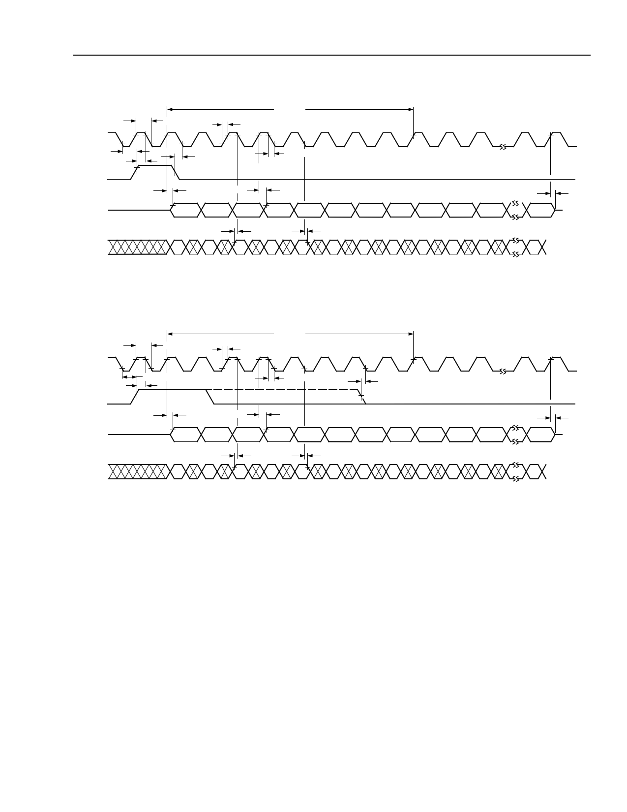
Timing Characteristics (continued)
tMCHMCL1
TIME SLOT
tMCH1MCH2
MCLK
1 2 3 4 5 6 7 8 9 10 11
tFSHMCL
FS
tMCLFSH
tFSLMCL
tMCL2MCL1
tMCHDV
tMCHDV1
Dx
CH 0
BIT 1
CH 0
BIT 2
CH 0
BIT 3
CH 0
BIT 4
CH 0
BIT 5
CH 0
BIT 6
CH 0
BIT 7
CH 0
BIT 8
CH 1
BIT 1
CH1
BIT 2
CH 1
BIT 3
tDVMCL
tMCLDV
DR
BIT
BIT
BIT BIT BIT
BIT BIT BIT
BIT BIT
BIT
1 2 3 4 5 6 78 1 2 3
DR
STABLE
DR
STABLE
Figure 5. Short FS Transmit and Receive Timing (Channel 0 First)
16
tMCHDZ
CH 1
BIT 8
BIT
8
5-3581.c
tMCHMCL1
TIME SLOT
tMCH1MCH2
MCLK
1 2 3 4 5 6 7 8 9 10 11
tFSHMCL
FS
tMCLFSH
tMCL2MCL1 tFSLMCL
tMCHDV
tMCHDV1
Dx
CH 1
BIT 1
CH 1
BIT 2
CH 1
BIT 3
CH 1
BIT 4
CH 1
BIT 5
CH 1
BIT 6
CH 1
BIT 7
CH 1
BIT 8
CH 0
BIT 1
CH0
BIT 2
CH 0
BIT 3
tDVMCL
tMCLDV
DR
BIT
BIT
BIT BIT BIT
BIT BIT BIT
BIT BIT
BIT
1 2 3 4 5 6 78 1 2 3
DR
STABLE
DR
STABLE
Figure 6. Long FS Transmit and Receive Timing (Channel 1 First)
16
tMCHDZ
CH 0
BIT 8
BIT
8
5-3581.d
Lucent Technologies Inc.
11
11 Page | ||
| Páginas | Total 16 Páginas | |
| PDF Descargar | [ Datasheet T7502.PDF ] | |
Hoja de datos destacado
| Número de pieza | Descripción | Fabricantes |
| T7502 | Dual PCM Codec | Agere Systems |
| Número de pieza | Descripción | Fabricantes |
| SLA6805M | High Voltage 3 phase Motor Driver IC. |
Sanken |
| SDC1742 | 12- and 14-Bit Hybrid Synchro / Resolver-to-Digital Converters. |
Analog Devices |
|
DataSheet.es es una pagina web que funciona como un repositorio de manuales o hoja de datos de muchos de los productos más populares, |
| DataSheet.es | 2020 | Privacy Policy | Contacto | Buscar |
