|
|
PDF NCP5173 Data sheet ( Hoja de datos )
| Número de pieza | NCP5173 | |
| Descripción | Boost Regulator | |
| Fabricantes | ON Semiconductor | |
| Logotipo | ||
Hay una vista previa y un enlace de descarga de NCP5173 (archivo pdf) en la parte inferior de esta página. Total 18 Páginas | ||
|
No Preview Available !
www.DataSheet4U.com
NCP5173
1.5 A 560 kHz−1.0 MHz
Boost Regulator
The NCP5173 is a switching regulator with a high efficiency, 1.5 A
integrated switch. It runs at a base frequency of 560 kHz and can be
synchronized to an external clock up to 1.0 MHz. This part operates
over a wide input voltage range, from 2.7 V to 30 V. The flexibility of
the design allows the chip to operate in most power supply
configurations, including boost, flyback, forward, inverting, and
SEPIC. The IC uses current mode architecture, which allows excellent
load and line regulation, as well as a practical means for limiting
current. Combining high frequency operation with a highly integrated
regulator circuit results in an extremely compact power supply
solution. The circuit design includes provisions for features such as
frequency synchronization, shutdown, and feedback controls for
positive voltage regulation.
Features
• Integrated Power Switch: 1.5 A Guaranteed
• Wide Input Range: 2.7 V to 30 V
• High Frequency Allows for Small Components
• Minimum External Components
• Easy External Synchronization
• Built−in Overcurrent Protection
• Frequency Foldback Reduces Component Stress During an
Overcurrent Condition
• Thermal Shutdown with Hysteresis
• Low 1.0 mm Maximum Profile
• Shut Down Current: 50 mA Maximum
Applications
• Flat Panel Displays
• Systems Requiring Low Profile Components
http://onsemi.com
5x6 QFN
MN SUFFIX
CASE 505AC
MARKING
DIAGRAM
1
NCP5173
AWLYYWW
NCP5173 = Specific Device Code
A = Assembly Location
WL = Wafer Lot
YY = Year
WW = Work Week
NOTE: Thermal pad is electrically isolated from IC
and all pins.
ORDERING INFORMATION
Device
NCP5173MN
NCP5173MNR2
Package
QFN
QFN
Shipping†
95 Units/Rail
2500 Tape & Reel
†For information on tape and reel specifications,
including part orientation and tape sizes, please
refer to our Tape and Reel Packaging Specification
Brochure, BRD8011/D.
© Semiconductor Components Industries, LLC, 2004
September, 2004 − Rev. 1
1
Publication Order Number:
NCP5173/D
1 page 
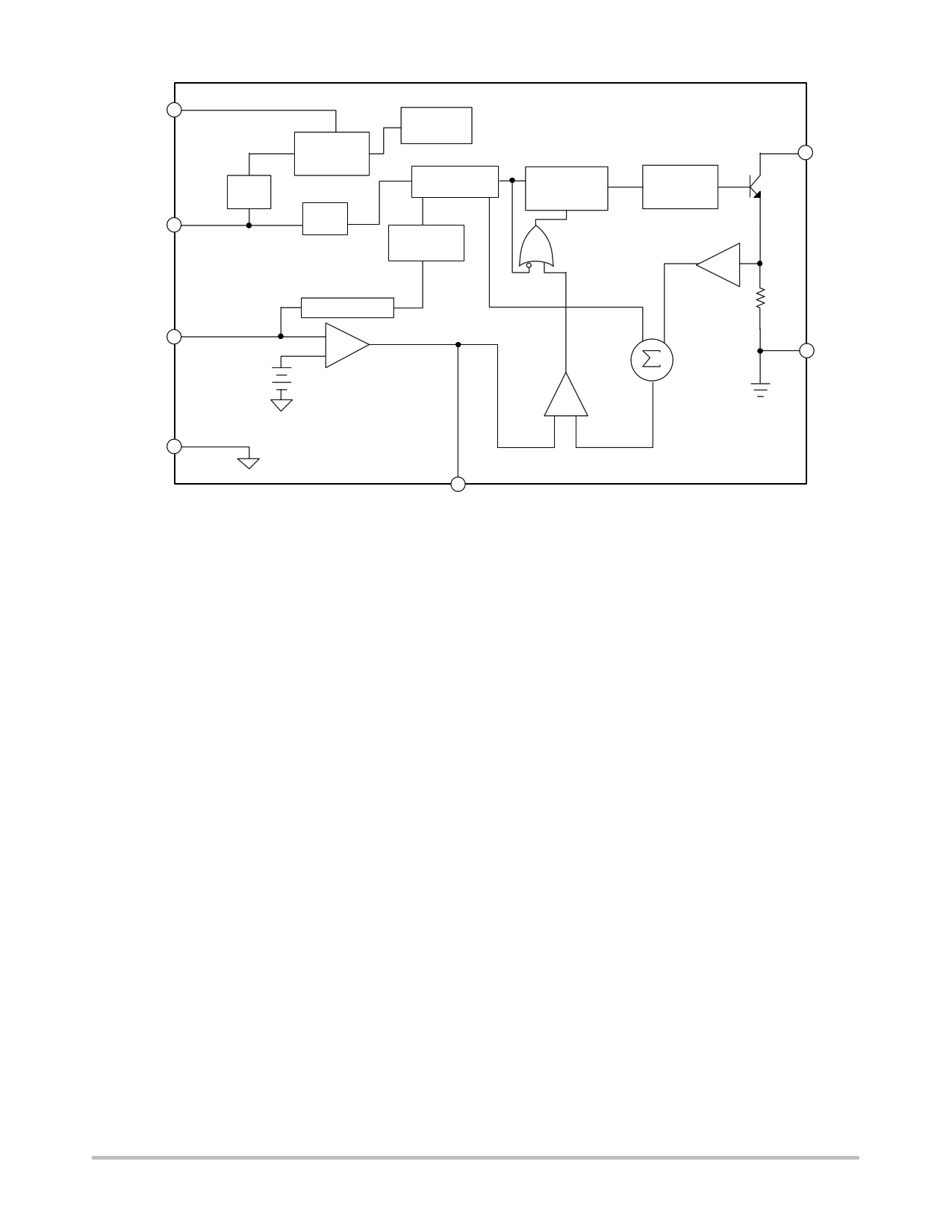
VCC
SS
FB
AGND
NCP5173
Shutdown
Delay
Timer
2.0 V
Regulator
Sync
Thermal
Shutdown
Oscillator
Frequency
Shift 5:1
1.276 V
0.4 V Detector
−
+
Positive
Error Amp
S
PWM
Latch
Q
R
Driver
VSW
Switch
Slope
Compensation
×5
PWM
Comparator
+−
Ramp
Summer
63 mW
PGND
VC
Figure 2. Block Diagram
http://onsemi.com
5
5 Page 
NCP5173
The low frequency pole, fP1, is determined by the error
amplifier output resistance and C1 as:
fP1
+
1
2pC1RO
The first zero generated by C1 and R1 is:
fZ1
+
1
2pC1R1
The phase lead provided by this zero ensures that the loop
has at least a 45° phase margin at the crossover frequency.
Therefore, this zero should be placed close to the pole
generated in the power stage which can be identified at
frequency:
fP
+
1
2pCORLOAD
where:
CO = equivalent output capacitance of the error amplifier
≈120 pF;
RLOAD= load resistance.
The high frequency pole, fP2, can be placed at the output
filter’s ESR zero or at half the switching frequency. Placing
the pole at this frequency will cut down on switching noise.
The frequency of this pole is determined by the value of C2
and R1:
fP2
+
1
2pC2R1
One simple method to ensure adequate phase margin is to
design the frequency response with a −20 dB per decade
slope, until unity−gain crossover. The crossover frequency
should be selected at the midpoint between fZ1 and fP2 where
the phase margin is maximized.
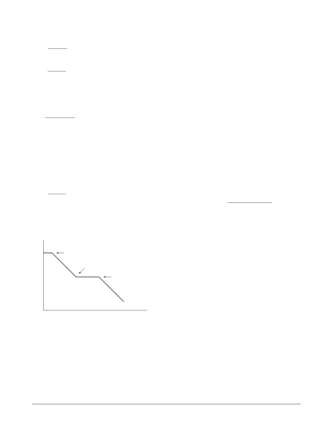
fP1
fZ1
fP2
Frequency (LOG)
Figure 26. Bode Plot of the Compensation Network
Shown in Figure 25
VSW Voltage Limit
In the boost topology, VSW pin maximum voltage is set by
the maximum output voltage plus the output diode forward
voltage. The diode forward voltage is typically 0.5 V for
Schottky diodes and 0.8 V for ultrafast recovery diodes:
VSW(MAX) + VOUT(MAX))VF
where:
VF = output diode forward voltage.
In the flyback topology, peak VSW voltage is governed by:
VSW(MAX) + VCC(MAX))(VOUT)VF) N
where:
N = transformer turns ratio, primary over secondary.
When the power switch turns off, there exists a voltage
spike superimposed on top of the steady−state voltage.
Usually this voltage spike is caused by transformer leakage
inductance charging stray capacitance between the VSW and
PGND pins. To prevent the voltage at the VSW pin from
exceeding the maximum rating, a transient voltage
suppressor in series with a diode is paralleled with the
primary windings. Another method of clamping switch
voltage is to connect a transient voltage suppressor between
the VSW pin and ground.
Magnetic Component Selection
When choosing a magnetic component, one must consider
factors such as peak current, core and ferrite material, output
voltage ripple, EMI, temperature range, physical size and
cost. In boost circuits, the average inductor current is the
product of output current and voltage gain (VOUT/VCC),
assuming 100% energy transfer efficiency. In continuous
conduction mode, inductor ripple current is:
IRIPPLE
+
VCC(VOUT * VCC)
(f)(L)(VOUT)
where:
f = 560 kHz
The peak inductor current is equal to average current plus
half of the ripple current, which should not cause inductor
saturation. The above equation can also be referenced when
selecting the value of the inductor based on the tolerance of
the ripple current in the circuits. Small ripple current
provides the benefits of small input capacitors and greater
output current capability. A core geometry like a rod or
barrel is prone to generating high magnetic field radiation,
but is relatively cheap and small. Other core geometries,
such as toroids, provide a closed magnetic loop to prevent
EMI.
Input Capacitor Selection
In boost circuits, the inductor becomes part of the input
filter, as shown in Figure 28. In continuous mode, the input
current waveform is triangular and does not contain a large
pulsed current, as shown in Figure 27. This reduces the
requirements imposed on the input capacitor selection.
During continuous conduction mode, the peak to peak
inductor ripple current is given in the previous section. As
we can see from Figure 27, the product of the inductor
current ripple and the input capacitor’s effective series
resistance (ESR) determine the VCC ripple. In most
applications, input capacitors in the range of 10 mF to
100 mF with an ESR less than 0.3 W work well up to a full
1.5 A switch current.
http://onsemi.com
11
11 Page | ||
| Páginas | Total 18 Páginas | |
| PDF Descargar | [ Datasheet NCP5173.PDF ] | |
Hoja de datos destacado
| Número de pieza | Descripción | Fabricantes |
| NCP5173 | Boost Regulator | ON Semiconductor |
| Número de pieza | Descripción | Fabricantes |
| SLA6805M | High Voltage 3 phase Motor Driver IC. |
Sanken |
| SDC1742 | 12- and 14-Bit Hybrid Synchro / Resolver-to-Digital Converters. |
Analog Devices |
|
DataSheet.es es una pagina web que funciona como un repositorio de manuales o hoja de datos de muchos de los productos más populares, |
| DataSheet.es | 2020 | Privacy Policy | Contacto | Buscar |
