|
|
|
PDF IDT23S08 Data sheet ( Hoja de datos )
| Número de pieza | IDT23S08 | |
| Descripción | 2.5V ZERO DELAY CLOCK MULTIPLIER | |
| Fabricantes | IDT | |
| Logotipo | ||
Hay una vista previa y un enlace de descarga de IDT23S08 (archivo pdf) en la parte inferior de esta página. Total 10 Páginas | ||
|
No Preview Available !
www.DataSheet4U.com
IDT23S08
3.3V ZERO DELAY CLOCK MULTIPLIER
COMMERCIAL AND INDUSTRIAL TEMPERATURE RANGES
3.3V ZERO DELAY CLOCK
MULTIPLIER, SPREAD
SPECTRUM COMPATIBLE
IDT23S08
FEATURES:
• Phase-Lock Loop Clock Distribution for Applications ranging
from 10MHz to 133MHz operating frequency
• Distributes one clock input to two banks of four outputs
• Separate output enable for each output bank
• External feedback (FBK) pin is used to synchronize the outputs
to the clock input
• Output Skew <200 ps
• Low jitter <200 ps cycle-to-cycle
• 1x, 2x, 4x output options (see table):
– IDT23S08-1 1x
– IDT23S08-2 1x, 2x
– IDT23S08-3 2x, 4x
– IDT23S08-4 2x
– IDT23S08-1H, -2H, and -5H for High Drive
• No external RC network required
• Operates at 3.3V VDD
• Spread spectrum compatible
• Available in SOIC and TSSOP packages
DESCRIPTION:
The IDT23S08 is a high-speed phase-lock loop (PLL) clock multiplier. It is
designed to address high-speed clock distribution and multiplication applica-
tions. The zero delay is achieved by aligning the phase between the incoming
clock and the output clock, operable within the range of 10 to 133MHz.
The IDT23S08 has two banks of four outputs each that are controlled via two
select addresses. By proper selection of input addresses, both banks can be
put in tri-state mode. In test mode, the PLL is turned off, and the input clock
directly drives the outputs for system testing purposes. In the absence of an
input clock, the IDT23S08 enters power down. In this mode, the device will
draw less than 12µA for Commercial Temperature range and less than25µA
for Industrial temperature range, and the outputs are tri-stated.
The IDT23S08 is available in six unique configurations for both pre-
scaling and multiplication of the Input REF Clock. (See available options
table.)
The PLL is closed externally to provide more flexibility by allowing the user
to control the delay between the input clock and the outputs.
The IDT23S08 is characterized for both Industrial and Commercial opera-
tion.
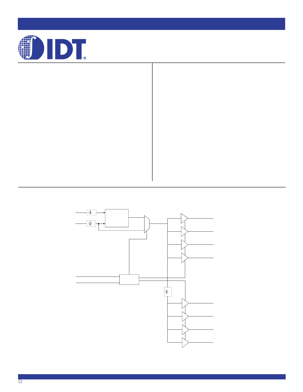
FUNCTIONAL BLOCK DIAGRAM
(-3, -4)
16
FBK
2
1
REF
2
(-5)
PLL
2
CLKA1
3
CLKA2
14
CLKA3
15
CLKA4
S2 8
S1 9
Control
Logic
(-2, -3) 2
6
CLKB1
7
CLKB2
10
CLKB3
11
CLKB4
The IDT logo is a registered trademark of Integrated Device Technology, Inc.
COMMERCIAL AND INDUSTRIAL
c 2003 Integrated Device Technology, Inc.
TEMPERATURE
1
RANGES
OCTOBER 2003
DSC 6394/8
1 page 
IDT23S08
3.3V ZERO DELAY CLOCK MULTIPLIER
COMMERCIAL AND INDUSTRIAL TEMPERATURE RANGES
SWITCHING CHARACTERISTICS - COMMERCIAL
Symbol Parameter
Conditions
t1 OutputFrequency
t1 OutputFrequency
t1 OutputFrequency
Duty Cycle = t2 ÷ t1
(-1, -2, -3, -4, -1H, -2H, -5H)
30pF Load, all devices
20pF Load, -1H, -2H, -5H Devices(1)
15pF Load, -1, -2, -3, -4 devices
Measured at 1.4V, FOUT = 66.66MHz
30pF Load
Duty Cycle = t2 ÷ t1
(-1, -2, -3, -4, -1H, -2H, -5H)
t3 Rise Time (-1, -2, -3, -4)
t3 Rise Time (-1, -2, -3, -4)
t3 Rise Time (-1H, -2H, -5H)
t4 Fall Time (-1, -2, -3, -4)
t4 Fall Time (-1, -2, -3, -4)
t4 Fall Time (-1H, -5H)
t5 Output to Output Skew on same Bank
(-1, -2, -3, -4)
Measured at 1.4V, FOUT = 50MHz
15pF Load
Measured between 0.8V and 2V, 30pF Load
Measured between 0.8V and 2V, 15pF Load
Measured between 0.8V and 2V, 30pF Load
Measured between 0.8V and 2V, 30pF Load
Measured between 0.8V and 2V, 15pF Load
Measured between 0.8V and 2V, 30pF Load
All outputs equally loaded
Output to Output Skew (-1H, -2H, -5H)
All outputs equally loaded
Output Bank A to Output Bank B (-1, -4, -2H, -5H) All outputs equally loaded
Output Bank A to Output Bank B Skew (-2, -3)
All outputs equally loaded
t6 Delay, REF Rising Edge to FBK Rising Edge
Measured at VDD/2
t7 Device to Device Skew
t8 Output Slew Rate
tJ Cycle to Cycle Jitter
(-1, -1H, -4, -5H)
Measured at VDD/2 on the FBK pins of devices
Measured between 0.8V and 2V on -1H, -2H, -5H
device using Test Circuit 2
Measured at 66.67 MHz, loaded outputs, 15pF Load
Measured at 66.67 MHz, loaded outputs, 30pF Load
tJ Cycle to Cycle Jitter
(-2, -2H, -3)
tLOCK PLL Lock Time
Measured at 133.3 MHz, loaded outputs, 15pF Load
Measured at 66.67 MHz, loaded outputs, 30pF Load
Measured at 66.67 MHz, loaded outputs, 15pF Load
Stable Power Supply, valid clocks presented
on REF and FBK pins
NOTE:
1. IDT23S08-5H has maximum input frequency of 133.33 MHz and maximum output of 66.67MHz.
Min. Typ. Max. Unit
10 — 100 MHz
10 — 133.3 MHz
10 — 133.3 MHz
40 50 60 %
45 50 55 %
— — 2.2 ns
— — 1.5 ns
— — 1.5 ns
— — 2.2 ns
— — 1.5 ns
— — 1.25 ns
— — 200 ps
— — 200 ps
— — 200 ps
— — 400 ps
— 0 ±250 ps
— 0 700 ps
1 — — V/ns
— — 200
— — 200 ps
— — 100
— — 400 ps
— — 400
— — 1 ms
5
5 Page | ||
| Páginas | Total 10 Páginas | |
| PDF Descargar | [ Datasheet IDT23S08.PDF ] | |
Hoja de datos destacado
| Número de pieza | Descripción | Fabricantes |
| IDT23S05 | 3.3V ZERO DELAY CLOCK BUFFER / SPREAD SPECTRUM COMPATIBLE | Integrated Device |
| IDT23S05-1DC | 3.3V ZERO DELAY CLOCK BUFFER / SPREAD SPECTRUM COMPATIBLE | Integrated Device |
| IDT23S05-1DCG | 3.3V ZERO DELAY CLOCK BUFFER / SPREAD SPECTRUM COMPATIBLE | Integrated Device |
| IDT23S05-1DCI | 3.3V ZERO DELAY CLOCK BUFFER / SPREAD SPECTRUM COMPATIBLE | Integrated Device |
| Número de pieza | Descripción | Fabricantes |
| SLA6805M | High Voltage 3 phase Motor Driver IC. |
Sanken |
| SDC1742 | 12- and 14-Bit Hybrid Synchro / Resolver-to-Digital Converters. |
Analog Devices |
|
DataSheet.es es una pagina web que funciona como un repositorio de manuales o hoja de datos de muchos de los productos más populares, |
| DataSheet.es | 2020 | Privacy Policy | Contacto | Buscar |